Diverse surface waves supported by bianisotropic meta surfaces
doi: 10.37188/CO.2021-0098
-
摘要: 基于结构化的金属表面,即超构表面,所获得的表面波最近得到了广泛关注。它们在各种不同的频率下在集成光学回路、成像以及生物检测中都有着良好的应用前景。本文中,我们展示了一种由双各向异性超构材料单元构成的超构表面可以支持多种不同偏振模式的表面态。这个结构拥有D2d点群对称性,包括了在xz和yz面内拥有镜面对称,以及在y = ±x方向上拥有C2旋转对称性。基于这种对称性,这个超构表面可以在kx和ky方向上支持横电模(TE)以及横磁模(TM)的同时支持在ky = ±kx方向上的纯纵模以及椭偏的横电磁模(TEM)。这种超构表面上的多种表面模式可能会产生新的表面波现象以及器件应用。Abstract: Surface waves supported by structured metallic surfaces, i.e.metasurfaces, have drawn wide attention recently.They are promising for various applications ranging from integrated photonic circuits to imaging and bio-sensing in various frequency regimes. In this work, we show that surface states with diverse polarization configurations can be supported by a metasurface consisting of a single layer of bianisotropic metamaterial elements.The structure possesses D2d symmetry, which includes mirror symmetry in the xz and yz plane, and C2 rotational symmetry along y = ±x axis. Due to this unique symmetry, the metasuface supports both transverse electric (TE) and transverse magnetic (TM) waves along kx and ky directions, while a purely longitudinal mode and an elliptically polarized transverse electromagnetic(TEM) mode along ky = ±kx directions. The versatility of the surface modes on the metasurface may lead to new surface wave phenomena and device applications.
-
Key words:
- surface plasmon /
- metasurface /
- bianisotropy /
- transverse electric /
- transverse magnetic
-
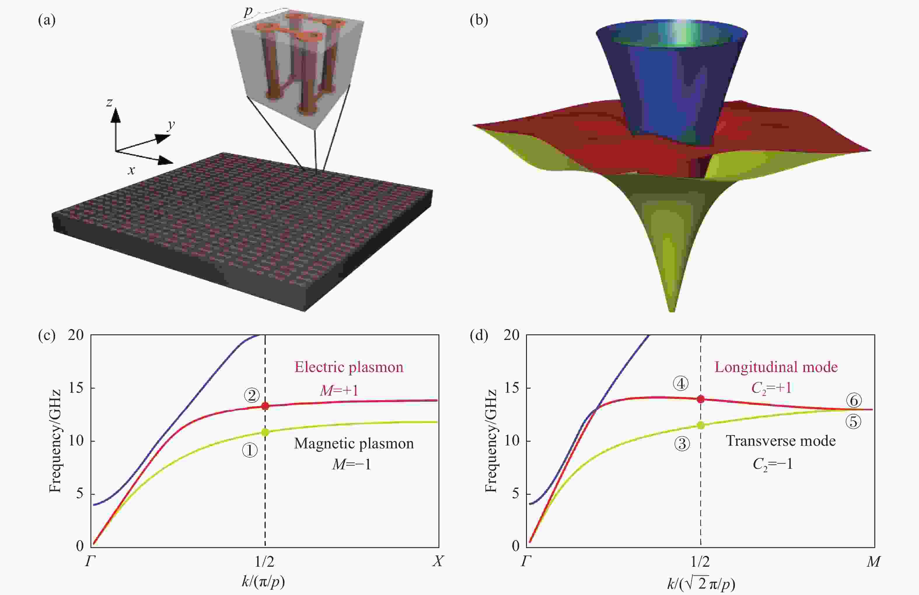
图 1 (a)单层超构表面示意图。每一个单元都由在介电常数为2.2的基底中的拥有D2d点群对称性的马鞍形金属内嵌物构成。该超构表面沿kx或ky方向的周期是p;(b)该表面的能带结构。第1、2、3条能带以及光锥分别由黄色、红色、蓝色以及绿色标出;(c)该超构表面沿着ky=0方向的色散。其中第1、2条能带在这个方向的模场分别是电等离子体激元以及磁等离子体激元;(d)该超构表面沿着ky=kx方向的色散。其中第1、2条能带在这个方向的模场分别是横电磁模(椭偏)以及纵模
Figure 1. (a) The schematic of the single-layer metasurface. Every unit cell consists of a saddle-shaped metallic inclusion possessing D2d point symmetry embedded in the dielectric substrate whose relative permittivity is 2.2. The period of the metasurface along kx or ky is p. (b) The band structure of the metasurface. The 1st, 2nd, 3rd bands and light cone are plotted in yellow, red, blue and green, respectively. (c) The dispersions of the surface modes along ky=0 direction. The modes along this direction corresponding to the 1st and 2nd bands can be regarded as electric plasmon and magnetic plasmon, respectively. (d) The dispersions of the surface modes along ky=kx direction. The modes along this direction for the 1st and 2nd bands can be regarded as transverse mode (elliptically polarized) and longitudinal mode, respectively
图 2 沿着x方向传播的表面等离子体激元的场分布。场分布所在截面的位置在最左边的结构单元示意图中标出;(a, b)在图1(c)中第1个模式上的点①处E和H分布;(c, d)在图1(c)中第2个模式上的点②处E和H分布。点①和②处的kx等于π/2p,p是沿x和y方向的结构周期
Figure 2. Field distributions of surface plasmon modes propagating along x direction. On the left, the schematic of the unit cell illustrating the plane in which the fields are plotted is shown. (a, b) The E and H field distributions for point ① on 1st mode in Fig. 1(c). (c, d) The E and H fields for point ② on 2nd mode. kx of point ① and ② is fixed at π/2p, where p is the period along x and y directions
图 3 沿kx=ky方向的表面等离子体激元模式的场分布。(a, b)图1(d)中第1个模式在点③处(kx=ky = π/2p)的场分布。仿真得到的在垂直传播方向的面上的E (a)和H (b)场分布,截面位置显示在上方示意图中。在两个图中,总体的场分布都在面内,证明了这是一个横电磁模。(c, d)图1(d)中第2个模式在点④处(kx=ky = π/2p)的场分布。仿真得到的在垂直传播方向的面上的E (c)和H (d)场分布,截面位置显示在上方示意图中。在两个图中,总体的场分布都指向面外(沿着传播方向),证明了这是一个同时拥有电场和磁场的纵模。(e-h)图1(d)中非常接近M点的⑤和⑥处的穿过结构单元中心的xy截面处的场分布,(e, f)分别代表了点⑤处的E和H场分布;(g, h)分别代表了点⑥处的E和H场分布。通过一个面内关于结构单元中心的90°旋转以及z方向上的镜面对称操作,这两个模式之间可以进行互相转换
Figure 3. Field distributions of surface plasmon modes propagating along kx=ky direction. (a, b) Field distributions of 1st mode at point ③ (kx=ky = π/2p) in Fig. 1(d). The simulated E (a) and H (b) field distributions in the plane perpendicular to the propagation direction, corresponding to the cutting plane shown in the schematic above. In both plots, the overall field distribution lie in the plane, indicating that this is a TEM mode. (c, d) Field distributions of 2nd mode at point ④ (kx=ky = π/2p) in Fig. 1(d). The simulated E (c) and H (d) field distributions in the plane perpendicular to the propagation direction, corresponding to the cutting plane shown in the schematic above. In both plots, the overall field distributions are out of plane (along the propagation direction), indicating that this is a pure longitudinal mode with both longitudinal components of E and H fields. (e-h) Field distributions of points ⑤ and ⑥ in Fig. 1(d), closing to the M point (phase advance is 170°), for a horizontal xy plane cutting through the center of the unit cell, as indicated by the schematic above. (e, f) correspond to the E and H field distributions of point ⑤, and (g, h) correspond to E and H field distributions of point ⑥. It is observed that the two modes are related to each other through an in-plane rotation of 90° about the center of the unit cell, followed by a mirror symmetry in z direction
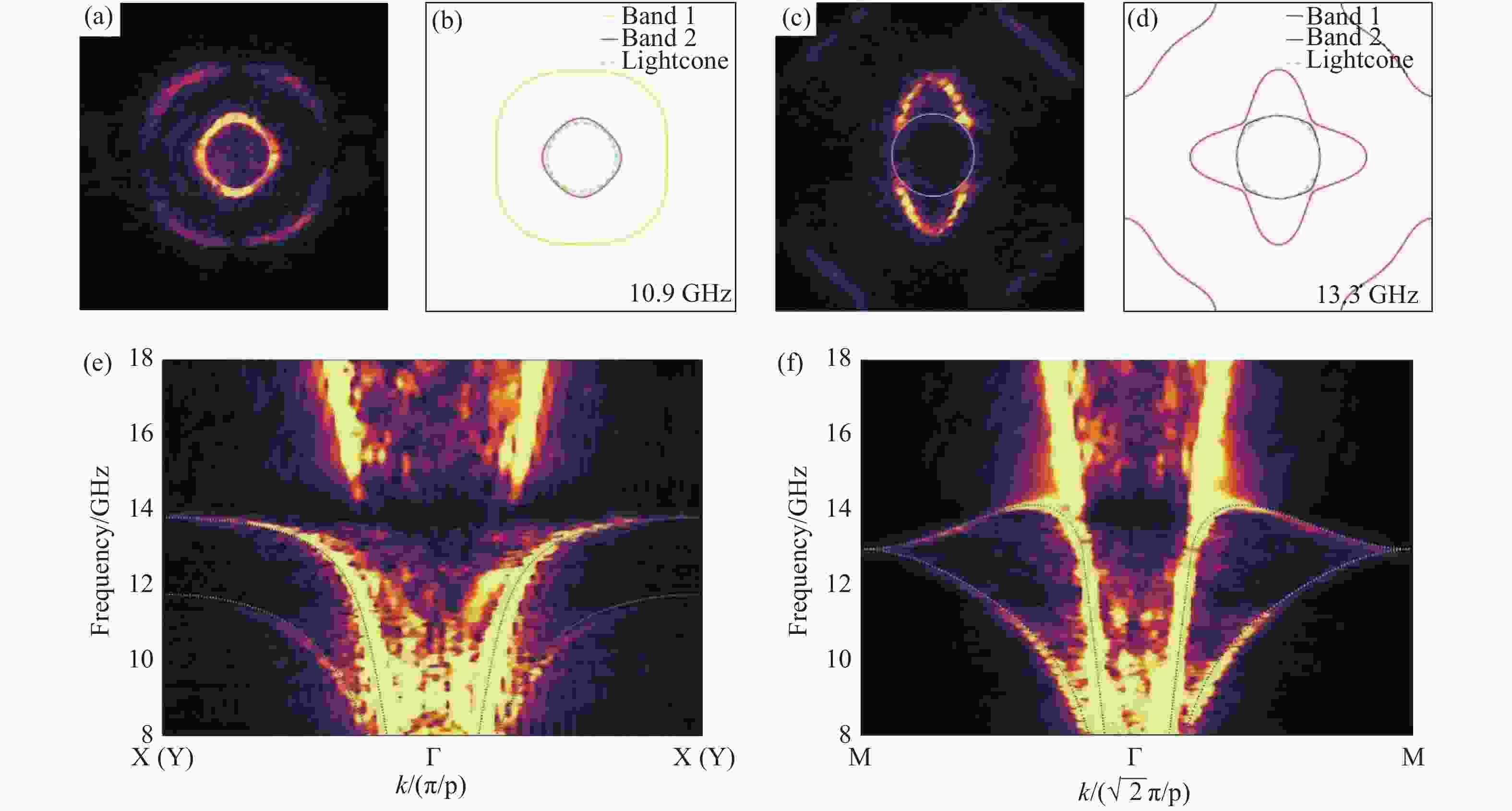
图 4 测量得到的表面模式的等频面以及色散曲线。测量(a)以及仿真(b)得到的在10.9 GHz处的等频面。测量(c)以及仿真(d)得到的在13.3 GHz处的等频面。(e, f)表面模式沿着kx/ky和kx=±ky方向上的色散曲线,虚线代表仿真结果
Figure 4. Measured EFC and dipersion curves of the surface modes. The measured (a) and simulated (b) EFC at frequency of 10.9 GHz. The measured (c) and simulated (d) EFC at frequency of 13.3 GHz. (e, f) The dispersion of the surface modes along kx/ky and kx=±ky directions, respectively. The dashed lines in the plots correspond to the simulation results
图 5 入射偏振依赖的表面模式激发的实验结果。(a)测量表面模式的实验设置。激发偶极天线的摆放方向或者垂直(上方示意图)或者水平(下方示意图);(b, c)上表面在px−pz或px+pz激发下的电场分布。(d, e)下表面在LCP或RCP激发下的电场分布。(b~e)所有的子图都代表了布里渊区等频面
Figure 5. Measurement of polarization controllable excitation of surface modes. (a) The experimental setup for measuring the surface mode. The excitation dipole antenna is oriented either in the vertical direction (upper panel) or the horizontal direction (lower panel). (b, c) Electric field distribution on top surfaces under polarization of px−pz and px+pz, respectively. (d, e) Same as (b, c) but the fields are measured on bottom surfaces under LCP and RCP excitation, respectively. All subplots attached to (b-e) are the corresponding EFCs in the Brillouin zone
-
[1] ZAYATS A V, SMOLYANINOV I I, MARADUDIN A A. Nano-optics of surface plasmon polaritons[J]. Physics Reports, 2005, 408(3-4): 131-314. doi: 10.1016/j.physrep.2004.11.001 [2] BARNES W L, DEREUX A, EBBESEN T W. Surface plasmon subwavelength optics[J]. Nature, 2003, 424(6950): 824-830. doi: 10.1038/nature01937 [3] PENDRY J B, MARTIN-MORENO L, GARCIA-VIDAL F J. Mimicking surface plasmons with structured surfaces[J]. Science, 2004, 305(5685): 847-848. doi: 10.1126/science.1098999 [4] HIBBINS A P, EVANS B R, SAMBLES J R. Experimental verification of designer surface plasmons[J]. Science, 2005, 308(5722): 670-672. doi: 10.1126/science.1109043 [5] GAN Q Q, FU ZH, DING Y J, et al. Ultrawide-band width slow-light system based on THz plasmonic graded metallic grating structures[J]. Physical Review Letters, 2008, 100(25): 256803. doi: 10.1103/PhysRevLett.100.256803 [6] GAN Q Q, DING Y J, BARTOLI F J. “Rainbow” trapping and releasing at telecommunication wavelengths[J]. Physical Review Letters, 2009, 102(5): 056801. doi: 10.1103/PhysRevLett.102.056801 [7] MAIER S A, ANDREWS S R, MARTÍN-MORENO L, et al. Terahertz surface plasmon-polariton propagation and focusing on periodically corrugated metal wires[J]. Physical Review Letters, 2006, 97(17): 176805. doi: 10.1103/PhysRevLett.97.176805 [8] ZHANG Y, XU Y H, TIAN CH X, et al. Terahertz spoof surface-plasmon-polariton subwavelength waveguide[J]. Photonics Research, 2018, 6(1): 18-23. doi: 10.1364/PRJ.6.000018 [9] XU W D, XIE L J, YING Y B. Mechanisms and applications of terahertz metamaterial sensing: a review[J]. Nanoscale, 2017, 9(37): 13864-13878. doi: 10.1039/C7NR03824K [10] SHALTOUT A M, SHALAEV V M, BRONGERSMA M L. Spatiotemporal light control with active metasurfaces[J]. Science, 2019, 364(6441): eaat3100. doi: 10.1126/science.aat3100 [11] ZHANG X Y, LI Q, LIU F F, et al. Controlling angular dispersions in optical metasurfaces[J]. Light:Science &Applications, 2020, 9(1): 76. [12] SUN SH L, HE Q, XIAO SH Y, et al. Gradient-index meta-surfaces as a bridge linking propagating waves and surface waves[J]. Nature Materials, 2012, 11(5): 426-431. doi: 10.1038/nmat3292 [13] NI X J, EMANI N K, KILDISHEV A V, et al. Broadband light bending with plasmonic nanoantennas[J]. Science, 2012, 335(6067): 427. doi: 10.1126/science.1214686 [14] HUANG L L, CHEN X ZH, MÜHLENBERND H, et al. Dispersionless phase discontinuities for controlling light propagation[J]. Nano Letters, 2012, 12(11): 5750-5755. doi: 10.1021/nl303031j [15] GENEVET P, CAPASSO F, AIETA F, et al. Recent advances in planar optics: from plasmonic to dielectric metasurfaces[J]. Optica, 2017, 4(1): 139-152. doi: 10.1364/OPTICA.4.000139 [16] MUELLER J P B, RUBIN N A, DEVLIN R C, et al. Metasurface polarization optics: independent phase control of arbitrary orthogonal states of polarization[J]. Physical Review Letters, 2017, 118(11): 113901. doi: 10.1103/PhysRevLett.118.113901 [17] DECKER M, STAUDE I, FALKNER M, et al. High-efficiency dielectric Huygens’ surfaces[J]. Advanced Optical Materials, 2015, 3(6): 813-820. doi: 10.1002/adom.201400584 [18] LIU L X, ZHANG X Q, KENNEY M, et al. Broadband metasurfaces with simultaneous control of phase and amplitude[J]. Advanced Materials, 2014, 26(29): 5031-5036. doi: 10.1002/adma.201401484 [19] GAO Y SH, FAN Y B, WANG Y J, et al. Nonlinear holographic all-dielectric metasurfaces[J]. Nano Letters, 2018, 18(12): 8054-8061. doi: 10.1021/acs.nanolett.8b04311 [20] LI G X, CHEN SH M, PHOLCHAI N, et al. Continuous control of the nonlinearity phase for harmonic generations[J]. Nature Materials, 2015, 14(6): 607-612. doi: 10.1038/nmat4267 [21] KOSHELEV K, TANG Y T, LI K F, et al. Nonlinear metasurfaces governed by bound states in the continuum[J]. ACS Photonics, 2019, 6(7): 1639-1644. doi: 10.1021/acsphotonics.9b00700 [22] KRASNOK A, TYMCHENKO M, ALÙ A. Nonlinear metasurfaces: a paradigm shift in nonlinear optics[J]. Materials Today, 2018, 21(1): 8-21. doi: 10.1016/j.mattod.2017.06.007 [23] YE W M, ZEUNER F, LI X, et al. Spin and wavelength multiplexed nonlinear metasurface holography[J]. Nature Communications, 2016, 7: 11930. doi: 10.1038/ncomms11930 [24] CHEN X ZH, HUANG L L, MÜHLENBERND H, et al. Dual-polarity plasmonic metalens for visible light[J]. Nature Communications, 2012, 3: 1198. doi: 10.1038/ncomms2207 [25] KHORASANINEJAD M, CHEN W T, DEVLIN R C, et al. Metalenses at visible wavelengths: diffraction-limited focusing and subwavelength resolution imaging[J]. Science, 2016, 352(6290): 1190-1194. doi: 10.1126/science.aaf6644 [26] WANG SH M, WU P C, SU V C, et al. A broadband achromatic metalens in the visible[J]. Nature Nanotechnology, 2018, 13(3): 227-232. doi: 10.1038/s41565-017-0052-4 [27] HUANG L L, CHEN X ZH, MÜHLENBERND H, et al. Three-dimensional optical holography using a plasmonic metasurface[J]. Nature Communications, 2013, 4: 2808. doi: 10.1038/ncomms3808 [28] LI L L, CUI T J, JI W, et al. Electromagnetic reprogrammable coding-metasurface holograms[J]. Nature Communications, 2017, 8(1): 197. doi: 10.1038/s41467-017-00164-9 [29] ZHENG G X, MÜHLENBERND H, KENNEY M, et al. Metasurface holograms reaching 80% efficiency[J]. Nature Nanotechnology, 2015, 10(4): 308-312. doi: 10.1038/nnano.2015.2 [30] TITTL A, LEITIS A, LIU M K, et al. Imaging-based molecular barcoding with pixelated dielectric metasurfaces[J]. Science, 2018, 360(6393): 1105-1109. doi: 10.1126/science.aas9768 [31] STAUDE I, SCHILLING J. Metamaterial-inspired silicon nanophotonics[J]. Nature Photonics, 2017, 11(5): 274-284. doi: 10.1038/nphoton.2017.39 [32] ZHANG SH, FAN W J, MINHAS B K, et al. Midinfrared resonant magnetic nanostructures exhibiting a negative permeability[J]. Physical Review Letters, 2005, 94(3): 037402. doi: 10.1103/PhysRevLett.94.037402 [33] YAO J, LIU ZH W, LIU Y M, et al. Optical negative refraction in bulk metamaterials of nanowires[J]. Science, 2008, 321(5891): 930. doi: 10.1126/science.1157566 [34] HENTSCHEL M, SCHÄFERLING M, DUAN X Y, et al. Chiral plasmonics[J]. Science Advances, 2017, 3(5): e1602735. doi: 10.1126/sciadv.1602735 [35] ZHANG SH, PARK Y S, LI J, et al. Negative refractive index in chiral metamaterials[J]. Physical Review Letters, 2009, 102(2): 023901. doi: 10.1103/PhysRevLett.102.023901 [36] KANG L, WANG CH Y, GUO X X, et al. Nonlinear chiral meta-mirrors: enabling technology for ultrafast switching of light polarization[J]. Nano Letters, 2020, 20(3): 2047-2055. doi: 10.1021/acs.nanolett.0c00007 [37] ASADCHY V S, DÍAZ-RUBIO A, TRETYAKOV S A. Bianisotropic metasurfaces: physics and applications[J]. Nanophotonics, 2018, 7(6): 1069-1094. doi: 10.1515/nanoph-2017-0132 [38] DORRAH A H, ELEFTHERIADES G V. Bianisotropic Huygens’ metasurface pairs for nonlocal power-conserving wave transformations[J]. IEEE Antennas and Wireless Propagation Letters, 2018, 17(10): 1788-1792. doi: 10.1109/LAWP.2018.2866874 [39] YAZDI M, ALBOOYEH M, ALAEE R. A bianisotropic metasurface with resonant asymmetric absorption[J]. IEEE Transactions on Antennas and Propagation, 2015, 63(7): 3004-3015. doi: 10.1109/TAP.2015.2423855 [40] WANG X CH, DÍAZ-RUBIO A, ASADCHY V S, et al. Extreme asymmetry in metasurfaces via evanescent fields engineering: angular-asymmetric absorption[J]. Physical Review Letters, 2018, 121(25): 256802. doi: 10.1103/PhysRevLett.121.256802 [41] GUO Q H, GAO W L, CHEN J, et al. Line degeneracy and strong spin-orbit coupling of light with bulk bianisotropic metamaterials[J]. Physical Review Letters, 2015, 115(6): 067402. doi: 10.1103/PhysRevLett.115.067402 [42] KHANIKAEV A B, MOUSAVI S H, TSE W K, et al. Photonic topological insulators[J]. Nature Materials, 2013, 12(3): 233-239. doi: 10.1038/nmat3520 [43] YANG B, GUO Q H, TREMAIN B, et al. Ideal Weyl points and helicoid surface states in artificial photonic crystal structures[J]. Science, 2018, 359(6379): 1013-1016. doi: 10.1126/science.aaq1221 [44] JIA H W, ZHANG R X, GAO W L, et al. Observation of chiral zero mode in inhomogeneous three-dimensional Weyl metamaterials[J]. Science, 2019, 363(6423): 148-151. doi: 10.1126/science.aau7707 [45] YANG B, BI Y G, ZHANG R X, et al. Momentum space toroidal moment in a photonic metamaterial[J]. Nature Communications, 2021, 12(1): 1784. doi: 10.1038/s41467-021-22063-w [46] PENG L, DUAN L F, WANG K W, et al. Transverse photon spin of bulk electromagnetic waves in bianisotropic media[J]. Nature Photonics, 2019, 13(12): 878-882. doi: 10.1038/s41566-019-0521-4 [47] XIA L B, YANG B, GUO Q H, et al. Simultaneous TE and TM designer surface plasmon supported by bianisotropic metamaterials with positive permittivity and permeability[J]. Nanophotonics, 2019, 8(8): 1357-1362. doi: 10.1515/nanoph-2019-0047 -


 下载:
下载:


