


-
摘要:铌酸锂薄膜调制器具有体积小、带宽高、半波电压低的优点,在光纤通讯和光纤传感领域具有重要应用价值,是近年来的研究热点。本文梳理了铌酸锂薄膜调制器的波导结构、耦合结构、电极结构的研究进展,总结了LN薄膜波导的制备工艺,并深入分析了不同结构调制器的性能。基于SOI和LNOI结构,薄膜调制器实现了 V π L<2 V∙cm,双锥形耦合方案实现了耦合损耗<0.5 dB/facet,行波电极结构实现了调制带宽>100 GHz。铌酸锂薄膜调制器的性能在大多数方面优于目前商用铌酸锂调制器,随着波导工艺进一步提升,将成为铌酸锂调制器的热门方案。最后对铌酸锂薄膜调制器的发展趋势和应用前景进行了展望。Abstract:Electro-optic modulators based on lithium niobate (LiNbO 3, LN) thin-film platforms are advantageous for their small volume, high bandwidth and low half-wave voltage. They have important application prospects in the field of optical fiber communication and optical fiber sensing, and thus have became a heavily researched topic in recent years. In this paper, the research progress of the waveguide structures, coupling structures and electrode structures of LN thin-film modulators are reviewed in detail. The fabrication process of a LN thin-film waveguide is summarized, and the performances of different modulator structures are analyzed. Based on SOI and LNOI, a platform modulator is realized with V π L<2 V∙cm, a bilayer inversely tapered coupling scheme achieves a coupling loss <0.5 dB/facet , and a traveling wave electrode structure achieves a modulation bandwidth >100 GHz. Thin-film LN modulators are better than commercial LN modulators in most aspects. It can be predicted that in the near future, with the further improvement in waveguide technology, thin-film LN will become a popular scheme of LN modulators. Finally, the potential directions for the future of their research are proposed.
-
Key words:
- lithium niobate thin-film/
- LNOI/
- electro-optic modulator
-
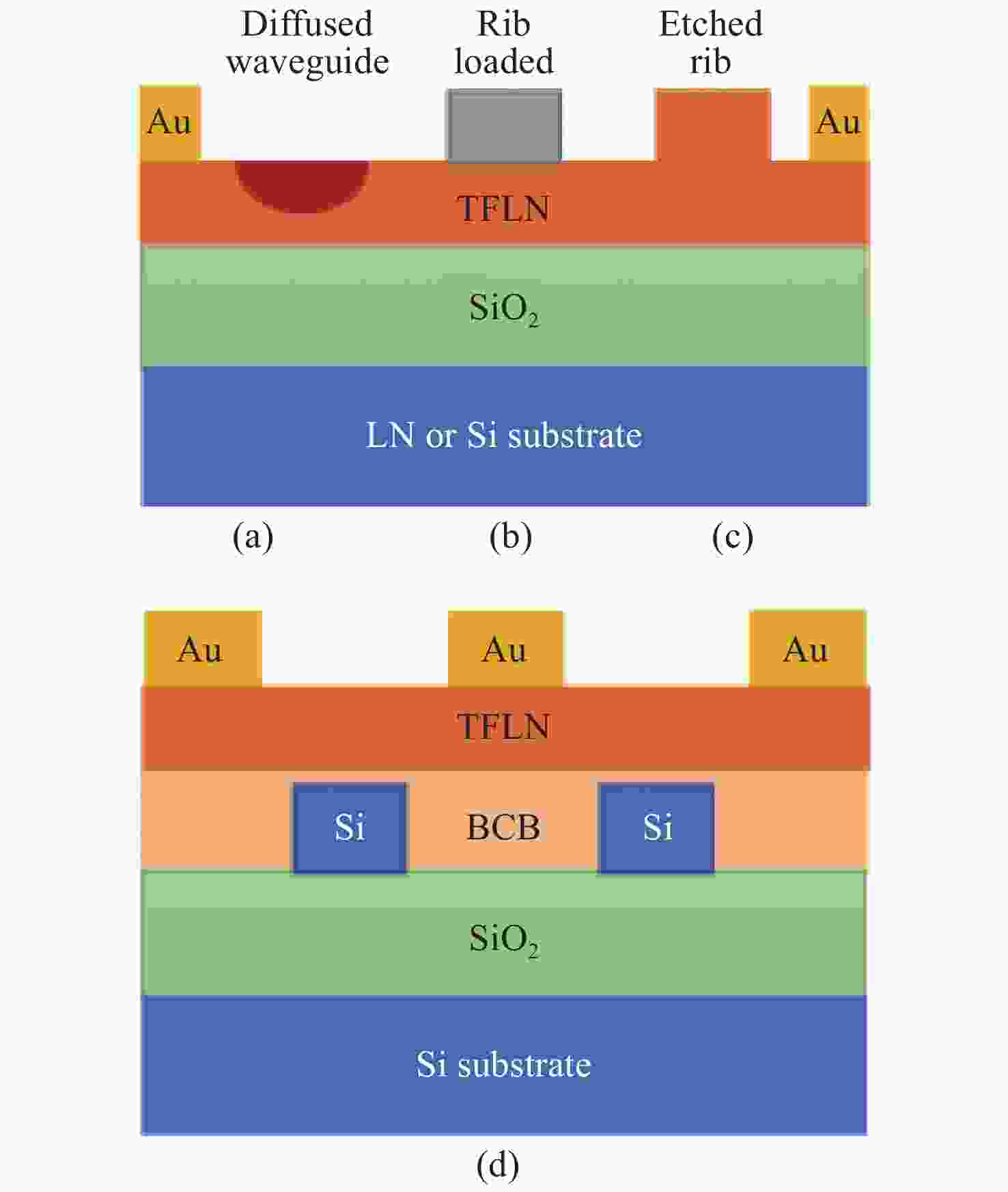
图 1(a)~(c)LNOI结构:(a)置换波导;(b)加载波导;(c)脊形波导。(d)SOI结构
Figure 1.(a)~(c) LNOI structure: (a) diffused waveguide; (b) loaded waveguide; (c) ridge waveguide. (d) SOI structure

图 2(a) MZI结构示意图;(b) MI结构示意图
Figure 2.Schematic diagrams of (a) MZI structure and (b) MI structure
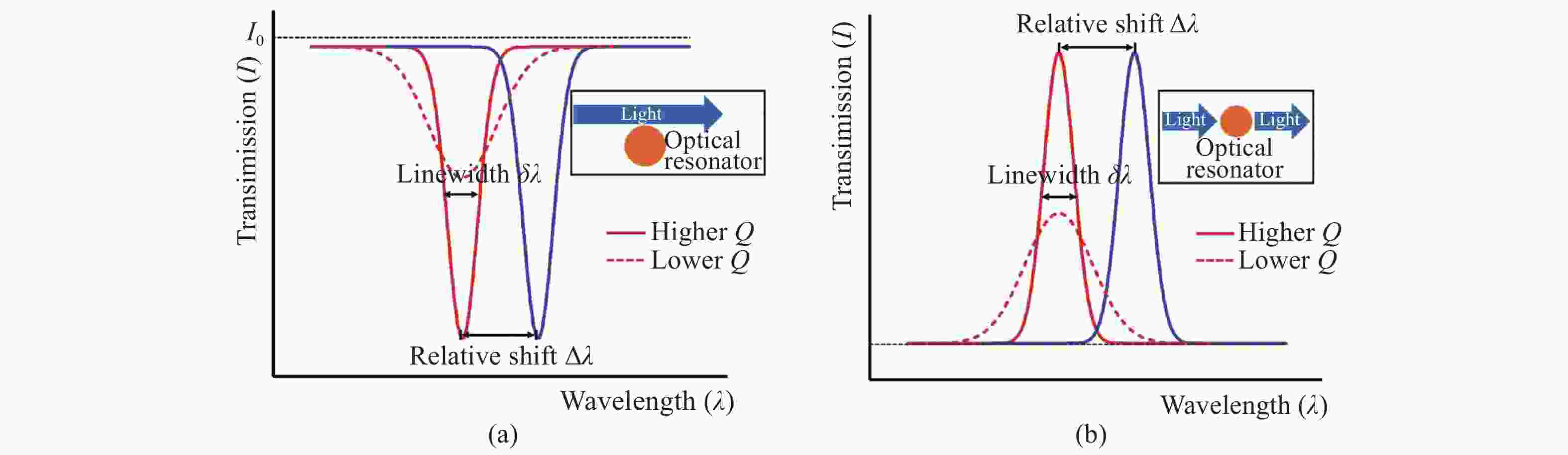
图 3两种谐振腔输出端口光强分布图[16]。(a)微环结构;(b)光子晶体结构。蓝线为施加电场后波导的光学特性变化曲线
Figure 3.Light intensity distribution diagram of the output port of the resonant cavity structure waveguide[16]. (a) Microring structure; (b) photonic crystal structure. The blue line is the optical characteristic change curve of the waveguide after an electric field is applied

图 6铌酸锂调制器中的电极基础结构。 (a)电场方向平行波导芯层;(b)电场方向垂直波导芯层
Figure 6.Electrode basic structure of LN modulators. (a) The electric field direction is parallel to the waveguide core; (b) the electric field direction is perpendicular to the waveguide core

图 7(a)集总电极结构;(b)行波电极结构
Figure 7.(a) Lumped electrode structure; (b) traveling wave electrode structure
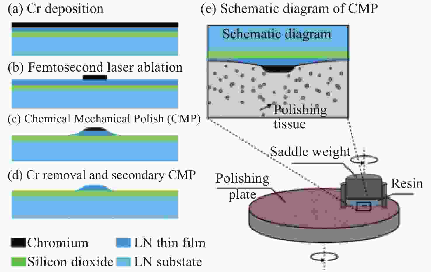
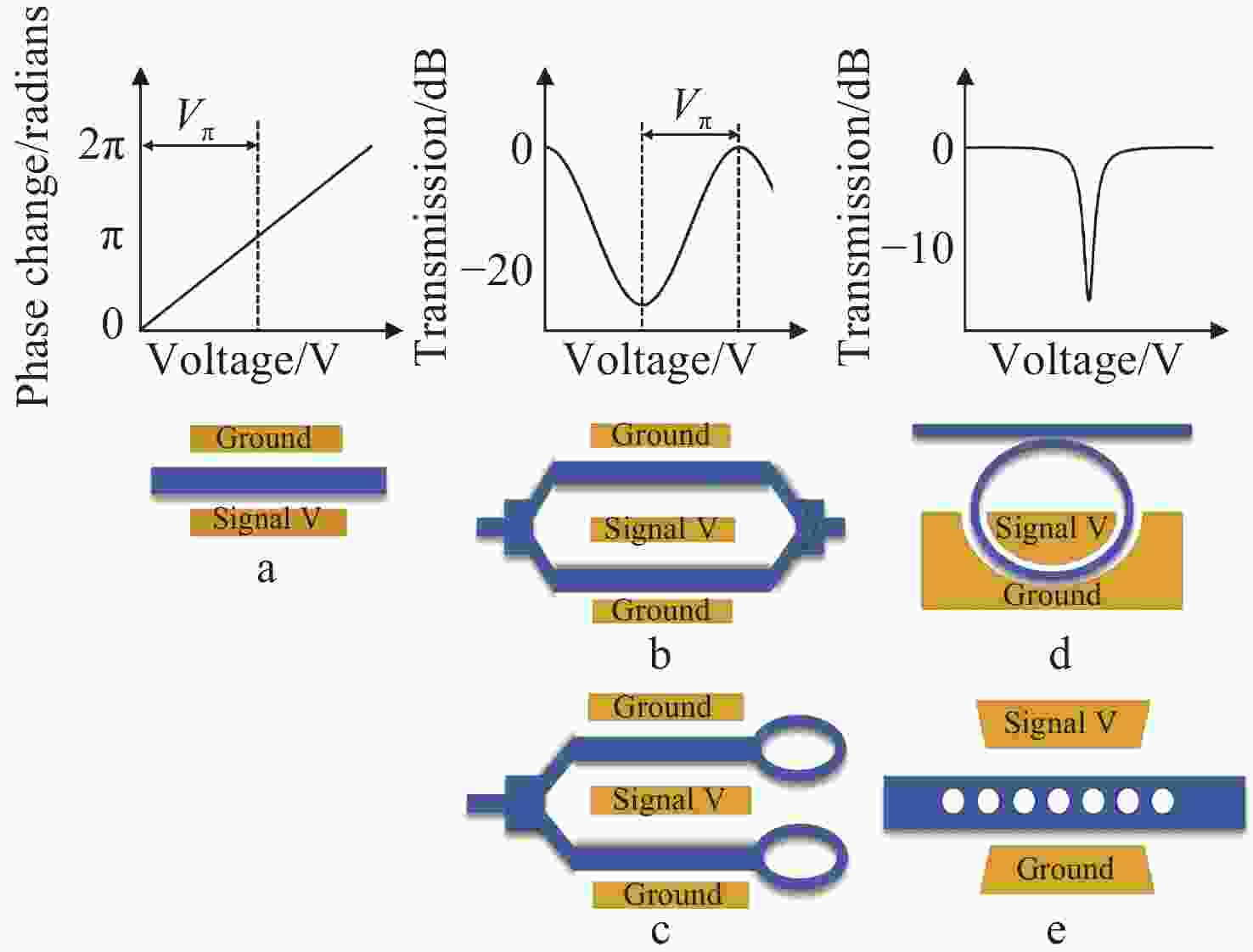
图 11调制器输出端口光场图。(a) PM;(b) MZM;(c) MIM;(d) MRM;(e) PHCM
Figure 11.The light field change diagram of the output port of the modulator. (a) PM; (b) MZM; (c) MIM; (d) MRM; (e) PHCM
表 2不同刻蚀工艺对比
Table 2.Comparison of different etching processes
刻蚀工艺 侧壁倾斜度 损耗/(dB·cm−1) 脊形宽度/μm 特点 湿法刻蚀[54] NAN $0.3\left({\rm{TE}}\right)$
$0.9\left({\rm{TM}}\right)$6.5 波导尺寸大 干法刻蚀[57] NAN $0.2\left({\rm{TE}}\right)$ 0.8 损耗小,波导尺寸小 化学机械抛光(CMP)[53,58] 9~51° $0.027\left({\rm{TE}}\right)$ 3 损耗小,波导尺寸大 金刚石切割[61] >65° $1.2\left({\rm{TE}}\right)$
$2.8\left({\rm{TM}}\right)$2.1 损耗较大,
波导容易断裂 下载:
导出CSV
下载:
导出CSV
表 4
${V}_{{\text{π}} }{L}$ 总结Table 4.
${V}_{{\text{π}} }{L}$ summary论文编号 调制器薄膜
结构分类调制器光学
结构分类${ V }_{ {\text{π} } }{L}/({\rm{V} }\cdot{\rm{ cm} }$) 年份 [70] Rib Etch on LNOI MZM 1.75 2021 [25] Rib Etch on LNOI MZM 2.36 2021 [62] Rib load on LNOI MZM 2.112 2020 [71] Rib load on LNOI MZM 3.12 2020 [72] Rib Etch on LNOI MZM 2.47/2.325 2020 [73] Rib Etch on LNOI MZM 2.2 2020 [74] Rib Etch on LNOI MZM 1.6 2019 [75] TFLN on SOI MZM 2.55 2019 [13] TFLN on SOI MZM 2.225 2019 [76] TFLN on SOI MIM 1.2 2019 [64] Rib load on LNOI MZM 3.6 2019 [64] Rib Etch on LNOI MZM 4.9 2019 [47] PE&APE on LNOI MZM 10.2 2019 [77] Rib Etch on LNOI MIM 1.4 2019 [12] TFLN on SOI MZM 6.7 2018 [49] Rib Etch on LNOI MZM 1.8 2018 [57] Rib Etch on LNOI MZM 2.8/2.3/2.2 2018 [78] PE&APE on LNOI PM 6.5 2016 下载:
导出CSV
表 6光学损耗总结
Table 6.Summary of optical loss
论文编号 调制器薄膜
结构分类调制器光学
结构分类光学损耗/dB 年份 [25] Rib Etch on LNOI MZM 3 2021 [62] Rib load on LNOI MZM 12.4 2020 [71] Rib load on LNOI MZM 13.86 2020 [79] Rib Etch on LNOI PHCM 2.2 2020 [72] Rib Etch on LNOI MZM 9.7/10.4 2020 [75] TFLN ON SOI MZM 2.5 2019 [13] TFLN ON SOI MZM <1 2019 [76] TFLN ON SOI MIM 3.3 2019 [77] Rib Etch on LNOI MIM 7.8 2019 [82] Rib load on LNOI PM >8.4 2016 下载:
导出CSV
表 83 dB带宽总结
Table 8.Summary of 3 dB bandwidth
论文编号 调制器薄膜
结构分类调制器光学
结构分类3 dB带宽/GHz 年份 [70] Rib Etch on LNOI MZM 40 2021 [25] Rib Etch on LNOI MZM 60 2021 [71] Rib load on LNOI MZM 29 2020 [79] Rib Etch on LNOI PHCM 17.5 2020 [72] Rib Etch on LNOI MZM 48/67 2020 [80] Rib Etch on LNOI MRM 28 2020 [73] Rib Etch on LNOI MZM 67 2020 [75] TFLN ON SOI MZM >70 2019 [13] TFLN ON SOI MZM 100 2019 [76] TFLN ON SOI MIM 17.5 2019 [64] Rib load on LNOI MZM 5~420 2019 [64] Rib Etch on LNOI MZM 3~340 2019 [83] Rib Etch on LNOI PM 30 2019 [77] Rib Etch on LNOI MIM 12 2019 [12] TFLN ON SOI MZM 100 2018 [49] Rib Etch on LNOI MRM 30 2018 [57] Rib Etch on LNOI MZM 15~80 2018 下载:
导出CSV
表 9调制速率总结
Table 9.Summary of modulation rate
论文编号 调制器薄膜
结构分类调制器光学
结构分类调制速率/(${\rm{Gbit}}{{\rm{s}}}^{-1}$) 年份 [71] Rib load on LNOI MZM 29@NRZ 2020 [72] Rib Etch on LNOI MZM 220@QPSK
320@QAM2020 [79] Rib Etch on LNOI PHCM 11@NRZ 2020 [75] TFLN ON SOI MZM 100@OOK
112@PAM-42019 [76] TFLN ON SOI MIM 40@OOK 2019 [77] Rib Etch on LNOI MIM 35@NRZ 2019 [49] Rib Etch on LNOI MRM 40@NRZ 2018 下载:
导出CSV
-
[1] WOOTEN E L, KISSA K M, YI-YAN A,et al. A review of lithium niobate modulators for fiber-optic communications systems[J].IEEE Journal of Selected Topics in Quantum Electronics, 2000, 6(1): 69-82.doi:10.1109/2944.826874 [2] TENG M, HONARDOOST A, ALAHMADI Y,et al. Miniaturized silicon photonics devices for integrated optical signal processors[J].Journal of Lightwave Technology, 2020, 38(1): 6-17.doi:10.1109/JLT.2019.2943251 [3] SUN CH, WADE M T, LEE Y,et al. Single-chip microprocessor that communicates directly using light[J].Nature, 2015, 528(7583): 534-538.doi:10.1038/nature16454 [4] OGISO Y, OZAKI J, UEDA Y,et al. Over 67 GHz bandwidth and 1.5 VVπInP-based optical IQ modulator with n-i-p-n heterostructure[J].Journal of Lightwave Technology, 2017, 35(8): 1450-1455.doi:10.1109/JLT.2016.2639542 [5] KOEBER S, PALMER R, LAUERMANN M,et al. Femtojoule electro-optic modulation using a silicon-organic hybrid device[J].Light:Science&Applications, 2015, 4(2): e255. [6] HAFFNER C, CHELLADURAI D, FEDORYSHYN Y,et al. Low-loss plasmon-assisted electro-optic modulator[J].Nature, 2018, 556(7702): 483-486.doi:10.1038/s41586-018-0031-4 [7] GUTIERREZ A M, GALAN J V, HERRERA J,et al. . High linear ring-assisted MZI electro-optic silicon modulators suitable for radio-over-fiber applications[C].Proceedings of the 9th International Conference on Group IV Photonics (GFP),IEEE, 2012: 57-59. [8] 陈柄言, 于永吉, 吴春婷, 等. 窄线宽1064 nm光纤 泵浦高效率中红外3.8 μm MgO: PPLN光参量振荡器[J]. 中国光学,2021,14(2):361-367.doi:10.37188/CO.2020-0169CHEN B Y, YU Y J, WU CH T,et al. High efficiency mid-infrared 3.8 μm MgO: PPLN optical parametric oscillator pumped by narrow linewidth 1064 nm fiber laser[J].Chinese Optics, 2021, 14(2): 361-367. (in Chinese)doi:10.37188/CO.2020-0169 [9] Srico. Lithium niobate modulator[EB/OL]. [2021-08-31].https://www.srico.com/products/. [10] Optilab. Lithium niobate modulator[EB/OL]. [2021-08-31].https://www.optilab.com/optical-modulator. [11] EOspace. Lithium niobate modulator[EB/OL]. [2021-08-31].https://www.eospace.com/product-summary-modulator. [12] WEIGEL P O, ZHAO J, FANG K,et al. Bonded thin film lithium niobate modulator on a silicon photonics platform exceeding 100 GHz 3-dB electrical modulation bandwidth[J].Optics Express, 2018, 26(18): 23728-23739.doi:10.1364/OE.26.023728 [13] WANG X X, WEIGEL P O, ZHAO J,et al. Achieving beyond-100-GHz large-signal modulation bandwidth in hybrid silicon photonics Mach Zehnder modulators using thin film lithium niobate[J].APL Photonics, 2019, 4(9): 096101.doi:10.1063/1.5115243 [14] LI M X, LIANG H X, LUO R,et al. High‐Q2D lithium niobate photonic crystal slab nanoresonators[J].Laser&Photonics Reviews, 2019, 13(5): 1800228. [15] LI M X, LIANG H X, LUO R,et al. Photon-level tuning of photonic nanocavities[J].Optica, 2019, 6(7): 860-863.doi:10.1364/OPTICA.6.000860 [16] QIAO Q F, XIA J, LEE C,et al. Applications of photonic crystal nanobeam cavities for sensing[J].Micromachines, 2018, 9(11): 541.doi:10.3390/mi9110541 [17] 李天琦, 毛小洁, 雷健, 等. 固体 器与光纤 器对光子晶体光纤棒耦合的分析与对比[J]. 中国光学,2018,11(6):958-973.doi:10.3788/co.20181106.0958LI T Q, MAO X J, LEI J,et al. Analysis and comparison of solid-state lasers and fiber lasers on the coupling of rod-type photonic crystal fiber[J].Chinese Optics, 2018, 11(6): 958-973. (in Chinese)doi:10.3788/co.20181106.0958 [18] 史光辉. 半导体 耦合新方法[J]. 中国光学,2013,6(3):343-352.SHI G H. Improved method for semiconductor laser coupling[J].Chinese Optics, 2013, 6(3): 343-352. (in Chinese) [19] SON G, HAN S, PARK J,et al. High-efficiency broadband light coupling between optical fibers and photonic integrated circuits[J].Nanophotonics, 2018, 7(12): 1845-1864.doi:10.1515/nanoph-2018-0075 [20] HONARDOOST A, GONZALEZ G F C, KHAN S,et al. Cascaded integration of optical waveguides with third-order nonlinearity with lithium niobate waveguides on silicon substrates[J].IEEE Photonics Journal, 2018, 10(3): 4500909. [21] LI Y, LAN T, LI J,et al. High-efficiency edge-coupling based on lithium niobate on an insulator wire waveguide[J].Applied Optics, 2020, 59(22): 6694-6701.doi:10.1364/AO.395897 [22] KRASNOKUTSKA I, TAMBASCO J L J, PERUZZO A. Nanostructuring of LNOI for efficient edge coupling[J].Optics Express, 2019, 27(12): 16578-16585.doi:10.1364/OE.27.016578 [23] LIU D N, FENG L SH, JIA Y Z,et al. Heterogeneous integration of LN and Si3N4waveguides using an optical interlayer coupler[J].Optics Communications, 2019, 436: 1-6.doi:10.1016/j.optcom.2018.11.058 [24] HE L Y, ZHANG M, SHAMS-ANSARI A,et al. Low-loss fiber-to-chip interface for lithium niobate photonic integrated circuits[J].Optics Letters, 2019, 44(9): 2314-2317.doi:10.1364/OL.44.002314 [25] YING P, TAN H Y, ZHANG J W,et al. Low-loss edge-coupling thin-film lithium niobate modulator with an efficient phase shifter[J].Optics Letters, 2021, 46(6): 1478-1481.doi:10.1364/OL.418996 [26] KRASNOKUTSKA I, CHAPMAN R J, TAMBASCO J L J,et al. High coupling efficiency grating couplers on lithium niobate on insulator[J].Optics Express, 2019, 27(13): 17681-17685.doi:10.1364/OE.27.017681 [27] MAHMOUD M, CAI L T, BOTTENFIELD C,et al. Lithium niobate electro-optic racetrack modulator etched in Y-Cut LNOI platform[J].IEEE Photonics Journal, 2018, 10(1): 6600410. [28] YAO N, ZHOU J X, GAO R H,et al. Efficient light coupling between an ultra-low loss lithium niobate waveguide and an adiabatically tapered single mode optical fiber[J].Optics Express, 2020, 28(8): 12416-12423.doi:10.1364/OE.391228 [29] WANG M K, LI J H, CHEN K X,et al. Thin-film lithium niobate electro-optic modulator on a D-shaped fiber[J].Optics Express, 2020, 28(15): 21464-21473.doi:10.1364/OE.396613 [30] ALFERNESS R C. Waveguide electrooptic modulators[J].IEEE Transactions on Microwave Theory and Techniques, 1982, 30(8): 1121-1137.doi:10.1109/TMTT.1982.1131213 [31] BINH L N. Tilted traveling wave electrodes and impacts on high-speed operation of integrated electro-optic modulators: modeling and experimental demonstration[J].Optical Engineering, 2009, 48(9): 097005.doi:10.1117/1.3231504 [32] YANG D C, CHEN Y K, XIANG M H,et al. Traveling wave electrode design for a LiNbO3integrated optical switch[J].Proceedings of SPIE, 2019, 11334: 113341B. [33] GEE A, JAAFAR A H, KEMP N T. Nanoscale junctions for single molecule electronics fabricated using bilayer nanoimprint lithography combined with feedback controlled electromigration[J].Nanotechnology, 2020, 31(15): 155203.doi:10.1088/1361-6528/ab6473 [34] AIDIL S A, NUZAIHAN M N M, ARSHAD M K,et al. . Fabrication and characterization of poly-Si nanowire with Thin Film of Ni/Au contact pad using conventional photolithography[C].Proceedings of 2019 IEEE International Conference on Sensors and Nanotechnology,IEEE, 2019: 29-32. [35] KUBOTA K, NODA J, MIKAMI O. Traveling wave optical modulator using a directional coupler LiNbO3waveguide[J].IEEE Journal of Quantum Electronics, 1980, 16(7): 754-760.doi:10.1109/JQE.1980.1070563 [36] LEVY M, RADOJEVIC A M. Single-crystal lithium niobate films by crystal ion slicing[M]. ALEXE M, GÖSELE U. Wafer Bonding: Applications and Technology. Berlin, Heidelberg: Springer, 2004: 417-450. [37] RAO A, FATHPOUR S. Compact lithium niobate electrooptic modulators[J].IEEE Journal of Selected Topics in Quantum Electronics, 2018, 24(4): 3400114. [38] HU H, GUI L, RICKEN R,et al. Towards nonlinear photonic wires in lithium niobate[J].Proceedings of SPIE, 2010, 7604: 76040R.doi:10.1117/12.842674 [39] POBERAJ G, KOECHLIN M, SULSER F,et al. Ion-sliced lithium niobate thin films for active photonic devices[J].Optical Materials, 2009, 31(7): 1054-1058.doi:10.1016/j.optmat.2007.12.019 [40] TAKIGAWA R, ASANO T. Thin-film lithium niobate-on-insulator waveguides fabricated on silicon wafer by room-temperature bonding method with silicon nanoadhesive layer[J].Optics Express, 2018, 26(19): 24413-24421.doi:10.1364/OE.26.024413 [41] HOWLADER M M R, SUGA T, KIM M J. Room temperature bonding of silicon and lithium niobate[J].Applied Physics Letters, 2006, 89(3): 031914.doi:10.1063/1.2229262 [42] LEE Y S, KIM G D, KIM W J,et al. Hybrid Si-LiNbO3microring electro-optically tunable resonators for active photonic devices[J].Optics Letters, 2011, 36(7): 1119-1121.doi:10.1364/OL.36.001119 [43] ARIZMENDI L. Photonic applications of lithium niobate crystals[J].Physica Status Solidi(A) , 2004, 201(2): 253-283.doi:10.1002/pssa.200303911 [44] YU J, ZHANG CH X, LI CH SH,et al. Influence of polarization-dependent crosstalk on scale factor in the in-line Sagnac interferometer current sensor[J].Optical Engineering, 2013, 52(11): 117101.doi:10.1117/1.OE.52.11.117101 [45] PAZ‐PUJALT G R, TUSCHEL D D, BRAUNSTEIN G,et al. Characterization of proton exchange lithium niobate waveguides[J].Journal of Applied Physics, 1994, 76(7): 3981-3987.doi:10.1063/1.358495 [46] PALIWAL A, SHARMA A, GUO R Y,et al. Electro-optic (EO) effect in proton-exchanged lithium niobate: towards EO modulator[J].Applied Physics B, 2019, 125(7): 115.doi:10.1007/s00340-019-7227-7 [47] HAN H P, XIANG B X, LIN T,et al. Design and optimization of proton exchanged integrated electro-optic modulators in X-Cut lithium niobate thin film[J].Crystals, 2019, 9(11): 549.doi:10.3390/cryst9110549 [48] ULLIAC G, GUICHARDAZ B, RAUCH J Y,et al. Ultra-smooth LiNbO3micro and nano structures for photonic applications[J].Microelectronic Engineering, 2011, 88(8): 2417-2419.doi:10.1016/j.mee.2011.02.024 [49] WANG CH, ZHANG M, STERN B,et al. Nanophotonic lithium niobate electro-optic modulators[J].Optics Express, 2018, 26(2): 1547-1555.doi:10.1364/OE.26.001547 [50] KRASNOKUTSKA I, TAMBASCO J L J, LI X J,et al. Ultra-low loss photonic circuits in lithium niobate on insulator[J].Optics Express, 2018, 26(2): 897-904.doi:10.1364/OE.26.000897 [51] WANG J, BO F, WAN SH,et al. High-Qlithium niobate microdisk resonators on a chip for efficient electro-optic modulation[J].Optics Express, 2015, 23(18): 23072-23078.doi:10.1364/OE.23.023072 [52] WANG M, WU R B, LIN J T,et al. Chemo‐mechanical polish lithography: a pathway to low loss large‐scale photonic integration on lithium niobate on insulator[J].Quantum Engineering, 2019, 1(1): e9.doi:10.1002/que2.9 [53] ZHANG J H, FANG ZH W, LIN J T,et al. Fabrication of crystalline microresonators of high quality factors with a controllable wedge angle on lithium niobate on insulator[J].Nanomaterials(Basel) , 2019, 9(9): 1218.doi:10.3390/nano9091218 [54] HU H, RICKEN R, SOHLER W,et al. Lithium niobate ridge waveguides fabricated by wet etching[J].IEEE Photonics Technology Letters, 2007, 19(6): 417-419.doi:10.1109/LPT.2007.892886 [55] ULLIAC G, CALERO V, NDAO A,et al. Argon plasma inductively coupled plasma reactive ion etching study for smooth sidewall thin film lithium niobate waveguide application[J].Optical Materials, 2016, 53: 1-5.doi:10.1016/j.optmat.2015.12.040 [56] 张琨, 岳远斌, 李彤, 等. 感应耦合等离子体刻蚀在聚合物光波导制作中的应用[J]. 中国光学,2012,5(1):64-70.doi:10.3969/j.issn.2095-1531.2012.01.010ZHANG K, YUE Y B, LI T,et al. Application of ICP etching in fabrication of polymer optical waveguide[J].Chinese Optics, 2012, 5(1): 64-70. (in Chinese)doi:10.3969/j.issn.2095-1531.2012.01.010 [57] WANG CH, ZHANG M, CHEN X,et al. Integrated lithium niobate electro-optic modulators operating at CMOS-compatible voltages[J].Nature, 2018, 562(7725): 101-104.doi:10.1038/s41586-018-0551-y [58] WU R B, WANG M, XU J,et al. Long low-loss-litium niobate on insulator waveguides with sub-nanometer surface roughness[J].Nanomaterials(Basel) , 2018, 8(11): 910.doi:10.3390/nano8110910 [59] LIN J T, XU Y X, FANG Z W,et al. Fabrication of high-Qlithium niobate microresonators using femtosecond laser micromachining[J].Scientific Reports, 2015, 5(1): 8072. [60] RÜTER C E, SUNTSOV S, KIP D,et al. Characterization of diced ridge waveguides in pure and Er-doped lithium-niobate-on-insulator (LNOI) substrates[J].Proceedings of SPIE, 2014, 8982: 89821G. [61] VOLK M F, SUNTSOV S, RÜTER C E,et al. Low loss ridge waveguides in lithium niobate thin films by optical grade diamond blade dicing[J].Optics Express, 2016, 24(2): 1386-1391.doi:10.1364/OE.24.001386 [62] AHMED A N R, NELAN S, SHI SH Y,et al. Subvolt electro-optical modulator on thin-film lithium niobate and silicon nitride hybrid platform[J].Optics Letters, 2020, 45(5): 1112-1115.doi:10.1364/OL.381892 [63] SOLER M, SCHOLTZ A, ZETO R,et al. Engineering photonics solutions for COVID-19[J].APL Photonics, 2020, 5(9): 090901.doi:10.1063/5.0021270 [64] HONARDOOST A, JUNEGHANI F A, SAFIAN R,et al. Towards subterahertz bandwidth ultracompact lithium niobate electrooptic modulators[J].Optics Express, 2019, 27(5): 6495-6501.doi:10.1364/OE.27.006495 [65] AHMED A N R, SHI SH Y, MERCANTE A J,et al. High-performance racetrack resonator in silicon nitride - thin film lithium niobate hybrid platform[J].Optics Express, 2019, 27(21): 30741-30751.doi:10.1364/OE.27.030741 [66] JIN T N, ZHOU J CH, LIN P T. Mid-infrared electro-optical modulation using monolithically integrated titanium dioxide on lithium niobate optical waveguides[J].Scientific Reports, 2019, 9(1): 15130.doi:10.1038/s41598-019-51563-5 [67] RABIEI P, MA J CH, KHAN S,et al. Heterogeneous lithium niobate photonics on silicon substrates[J].Optics Express, 2013, 21(21): 25573-25581.doi:10.1364/OE.21.025573 [68] RAO A, PATIL A, CHILES J,et al. Heterogeneous microring and Mach-Zehnder modulators based on lithium niobate and chalcogenide glasses on silicon[J].Optics Express, 2015, 23(17): 22746-22752.doi:10.1364/OE.23.022746 [69] LI SH, CAI L T, WANG Y W,et al. Waveguides consisting of single-crystal lithium niobate thin film and oxidized titanium stripe[J].Optics Express, 2015, 23(19): 24212-24219.doi:10.1364/OE.23.024212 [70] LIU Y, LI H, LIU J,et al. LowVπthin-film lithium niobate modulator fabricated with photolithography[J].Optics Express, 2021, 29(5): 6320-6329.doi:10.1364/OE.414250 [71] AHMED A N R, SHI SH Y, MERCANTE A,et al. High-efficiency lithium niobate modulator forKband operation[J].APL Photonics, 2020, 5(9): 091302.doi:10.1063/5.0020040 [72] XU M Y, HE M B, ZHANG H G,et al. High-performance coherent optical modulators based on thin-film lithium niobate platform[J].Nature Communications, 2020, 11(1): 3911.doi:10.1038/s41467-020-17806-0 [73] HAN H P, XIANG B X. Integrated electro-optic modulators inx-cut lithium niobate thin film[J].Optik, 2020, 212: 164691.doi:10.1016/j.ijleo.2020.164691 [74] DESIATOV B, SHAMS-ANSARI A, ZHANG M,et al. Ultra-low-loss integrated visible photonics using thin-film lithium niobate[J].Optica, 2019, 6(3): 380-384.doi:10.1364/OPTICA.6.000380 [75] HE M B, XU M Y, REN Y X,et al. High-performance hybrid silicon and lithium niobate Mach–Zehnder modulators for 100 Gbit s−1and beyond[J].Nature Photonics, 2019, 13(5): 359-364.doi:10.1038/s41566-019-0378-6 [76] XU M Y, CHEN W J, HE M B,et al. Michelson interferometer modulator based on hybrid silicon and lithium niobate platform[J].APL Photonics, 2019, 4(10): 100802.doi:10.1063/1.5115136 [77] JIAN J, XU M Y, LIU L,et al. High modulation efficiency lithium niobate Michelson interferometer modulator[J].Optics Express, 2019, 27(13): 18731-18739.doi:10.1364/OE.27.018731 [78] CAI L T, KANG Y, HU H. Electric-optical property of the proton exchanged phase modulator in single-crystal lithium niobate thin film[J].Optics Express, 2016, 24(5): 4640-4647.doi:10.1364/OE.24.004640 [79] LI M X, LING J W, HE Y,et al. Lithium niobate photonic-crystal electro-optic modulator[J].Nature Communications, 2020, 11(1): 4123.doi:10.1038/s41467-020-17950-7 [80] BAHADORI M, YANG Y S, HASSANIEN A E,et al. Ultra-efficient and fully isotropic monolithic microring modulators in a thin-film lithium niobate photonics platform[J].Optics Express, 2020, 28(20): 29644-29661.doi:10.1364/OE.400413 [81] KRASNOKUTSKA I, TAMBASCO J L J, PERUZZO A. Tunable large free spectral range microring resonators in lithium niobate on insulator[J].Scientific Reports, 2019, 9(1): 11086.doi:10.1038/s41598-019-47231-3 [82] JIN SH L, XU L T, ZHANG H H,et al. LiNbO3Thin-film modulators using silicon nitride surface ridge waveguides[J].IEEE Photonics Technology Letters, 2016, 28(7): 736-739.doi:10.1109/LPT.2015.2507136 [83] REN T H, ZHANG M, WANG CH,et al. An integrated low-voltage broadband lithium niobate phase modulator[J].IEEE Photonics Technology Letters, 2019, 31(11): 889-892.doi:10.1109/LPT.2019.2911876 -

 下载:
下载:


 点击查看大图

计量
- 文章访问数:3990
- HTML全文浏览量:3190
- PDF下载量:1395
- 被引次数:0
