Photonic-integrated interferometric array field-of-view splicing subaperture optical path design
-
摘要:
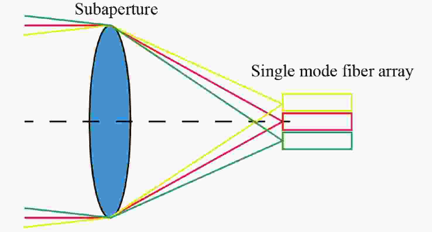
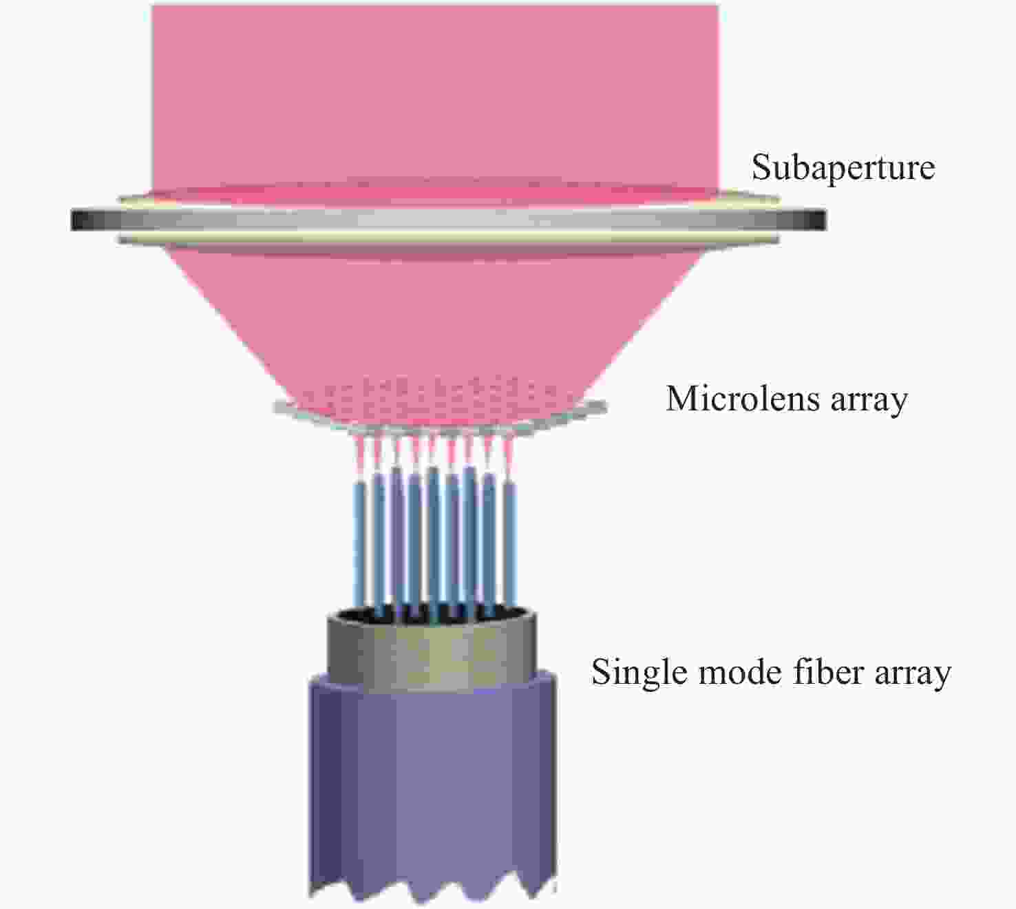
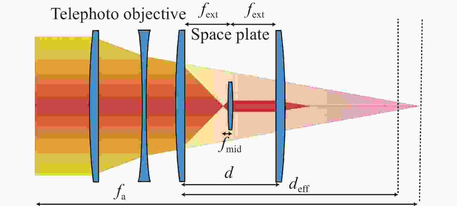
光子集成干涉成像系统一般是在子孔径焦平面处加单模光纤阵列,通过接收不同视场角的光束完成大视场拼接成像,但直接采用光纤阵列会导致成像视场不连续、子孔径焦距变长、厚度大幅度增加。针对以上问题,本文提出了一种结合微透镜阵列和光纤阵列对子孔径像面细分的方法以实现视场无缝拼接,并通过摄远物镜和三透镜空间压缩板组合大幅度降低了子孔径阵列的整体厚度。设计结果表明:通过在光纤阵列前加65×65的微透镜阵列对光束进行二次聚焦能够实现系统视场无缝拼接,视场扩大65倍后,全视场为
0.0489 °;可见光入射时单模光纤阵列中各光纤中心空间光耦合效率不低于40%;在加入空间压缩板压缩自由空间光路后,系统的整体厚度压缩了1个数量级。该系统在实现光子集成干涉成像系统大视场无缝拼接成像的同时,为解决超长焦距镜头过厚的问题提供了新的思路。Abstract:The photonic integrated interferometric imaging system generally adds single-mode fiber arrays at the focal plane of the subaperture and completes the large-field-of-view splicing imaging by receiving beams with different field-of-view angles. However, the direct use of fiber arrays leads to discontinuity of the imaging field-of-view and causes the focal length of the subaperture to lengthen, and the thickness is increased substantially. To address the above problems, we propose a combination of microlens arrays and fiber optic arrays to subdivide the subaperture image plane to achieve a seamless splicing of the field-of-view, and to significantly reduces the overall thickness of the subaperture array through the combination of the telephoto objective lens and the three-lens spatial compression plate. The design results show that by adding 65×65 microlens array in front of the fiber array to focus the beam twice to achieve the system field of view seamless splicing, the field of view is expanded 65 times, the full field of view is
0.0489 °, the efficiency of spatial optical coupling in the center of each fiber in the single-mode fiber array is not less than 40% when the visible light is incident, and after adding the spatial compression plate to compress the free-space light path, the overall thickness of the system achieves one order of magnitude compression. This design realizes photonic integrated interference imaging system large field of view seamless splicing imaging at the same time, provides a new way for the solution of the problem of excessive thickness in ultra-long focal length lenses.-
Key words:
- optical design /
- synthetic aperture /
- long focal length /
- visible-light imaging /
- fiber optic coupling
-
表 1 子孔径设计参数
Table 1. Subaperture design parameters
Parameters Specifications Wavelength/nm 400−680 Field-of-view 2w/° 0.04809 F-number 200.8 Focal length/mm − 9680.54 Total length/mm 478.98 Compression ratio 17.6 Telephoto ratio 0.0495 Back focal length/mm 30 表 2 单模光纤阵列参数
Table 2. Single-mode fiber array parameters
Parameters Specifications Array number 65×65 Core diameter/μm 3 Cladding diameter/μm 125 Numerical aperture 0.12 Operating wavelength/nm 400~680 mode field diameter/um
(1/e2fit – near field)3.3@405 nm
4.6@630 μm表 3 微透镜阵列参数
Table 3. Microlens array parameters
Parameters Specifications Array number 65×65 Subunit shape Square materials Fused silica Focal length/mm 0.523 Thickness/mm 0.5 Microlens pitch/μm 125 表 4 系统参数
Table 4. System parameters
Parameters Specifications Wavelength/nm 400~680 Field-of-view 2w/° 0.04809 F-number 5.2 Focal length/mm −250.923 Total length/mm 459.663 Numerical Aperture 0.0958 表 5 各视场光纤耦合效率
Table 5. Fiber coupling efficiency of each field of view
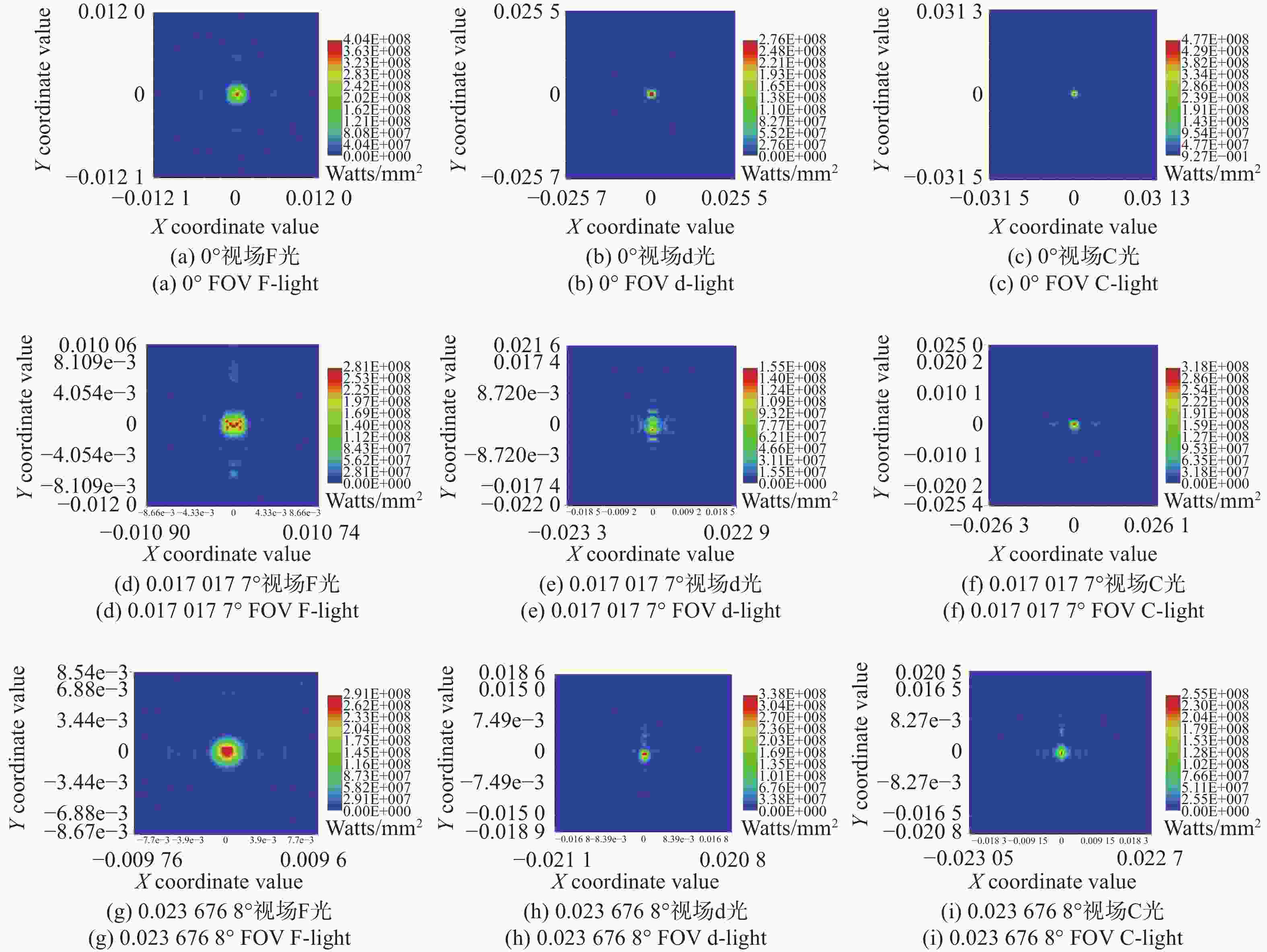
Field of view F d C 0° 0.565365 0.444582 0.450298 0.0170177 °0.587243 0.404386 0.481939 0.0236768 °0.610009 0.424886 0.451323 表 6 子孔径公差
Table 6. Tolerance of subaperture
Parameters Specifications Surface radius/mm ±0.02 Thickness/mm ±0.02 Surface decenter/mm ±0.02 Surface tilt/° ±0.01 Element decenter/mm ±0.05 Element tilt/° ±0.02 表 7 子孔径公差分析结果
Table 7. Tolerance analysis result of subaperture
Parameters Specifications The average MTF 0.35209144 MTF value of 98% > 0.21276278 MTF value of 90% > 0.27879303 MTF value of 80%° > 0.31568496 MTF value of 50% > 0.36178363 MTF value of 20% > 0.39748697 MTF value of 10% > 0.40812805 MTF value of 2% > 0.42106348 表 8 光纤耦合机械位置容差
Table 8. Mechancial position tolerance of fiber coupling
Parameters Specifications Longitudinal tolerance/mm ±0.025 Transvers tolerance/μm 0.711 angular deviation/° ±3 -
[1] BORN M, WOLF E. Principles of Optics: Electromagnetic Theory of Propagation, Interference and Diffraction of Light[M]. 7th ed. Cambridge: Cambridge University Press, 1999. [2] 苏云, 葛婧菁, 王业超, 等. 航天高分辨率对地光学遥感载荷研究进展[J]. 中国光学(中英文),2023,16(2):258-282. doi: 10.37188/CO.2022-0085SU Y, GE J J, WANG Y CH, et al. Research progress on high-resolution imaging system for optical remote sensing in aerospace[J]. Chinese Optics, 2023, 16(2): 258-282. (in Chinese). doi: 10.37188/CO.2022-0085 [3] KENDRICK R, DUNCAN A, WILM J, et al. Flat panel space based space surveillance sensor[C]. Proceedings of the Advanced Maui Optical and Space Surveillance Technologies Conference, 2013. [4] BADHAM K, KENDRICK R L, WUCHENICH D, et al. Photonic integrated circuit-based imaging system for SPIDER[C]. Proceedings of 2017 Conference on Lasers and Electro-Optics Pacific Rim (CLEO-PR), IEEE, 2017: 1-5. [5] DUNCAN A, KENDRICK R, THURMAN S, et al. SPIDER: next generation chip scale imaging sensor[C]. Proceedings of the Advanced Maui Optical and Space Surveillance Technologies Conference, 2015: 27. [6] SCOTT R P, SU T H, OGDEN C, et al. Demonstration of a photonic integrated circuit for multi-baseline interferometric imaging[C]. Proceedings of 2014 IEEE Photonics Conference, IEEE, 2014: 1-2. [7] CHEN H, ON M B, YUN-JHU-LEE, et al. Photonic interferometric imager with monolithic silicon CMOS photonic integrated circuits[C]. Optical Fiber Communication Conference 2022, Optica Publishing Group, 2022: Tu2I. 2. [8] GAO W P, YUAN Y, WANG X R, et al. Quantitative analysis and optimization design of the segmented planar integrated optical imaging system based on an inhomogeneous multistage sampling lens array[J]. Optics Express, 2021, 29(8): 11869-11884. doi: 10.1364/OE.421298 [9] WANG K, ZHU Y Q, AN Q CH, et al. Even sampling photonic-integrated interferometric array for synthetic aperture imaging[J]. Optics Express, 2022, 30(18): 32119-32128. doi: 10.1364/OE.468499 [10] 于海滨, 陈蓓曦, 潘枝峰, 等. 光子集成干涉成像系统微透镜排布设计与图像复原[J]. 应用光学,2022,43(2):213-220. doi: 10.5768/JAO202243.0201005YU H B, CHEN B X, PAN ZH F, et al. Arrangement of microlens and image restoration technology of photon integrated interferometric imaging system[J]. Journal of Applied Optics, 2022, 43(2): 213-220. (in Chinese). doi: 10.5768/JAO202243.0201005 [11] CHEN T B, ZENG X F, ZHANG ZH Y, et al. REM: a simplified revised entropy image reconstruction for photonics integrated interference imaging system[J]. Optics Communications, 2021, 501: 127341. doi: 10.1016/j.optcom.2021.127341 [12] GOODMAN J W. Statistical Optics[M]. Hoboken: John Wiley & Sons, 2015. [13] GUYON O. Wide field interferometric imaging with single-mode fibers[J]. Astronomy & Astrophysics, 2002, 387(1): 366-378. [14] RUILIER C. Degraded light coupling into single-mode fibers[J]. Proceedings of SPIE, 1998, 3350: 319-329. doi: 10.1117/12.317094 [15] SORENSEN N J, WEIL M T, LUNDEEN J S. Large-scale optical compression of free-space using an experimental three-lens spaceplate[J]. Optics Express, 2023, 31(12): 19766-19776. doi: 10.1364/OE.487255 -


 下载:
下载:
