


Design of high-speed MUTC-PD with electric field regulation layer
doi: 10.37188/CO.EN-2024-0030
-
摘要:
本文提出了一种具有电场调控层的新型改进型单行载流子光探测器(MUTC-PD)。该光探测器中,崖层后新增的p型掺杂电场调控层能够优化收集层中的电场强度,使光生电子在收集层中以峰值漂移速度输运;同时能够增强耗尽吸收层中的电场强度,优化其中光生载流子饱和速度输运特性;并且,器件收集层中光生电子的峰值漂移速度输运特性可以进一步优化其寄生电容特性,从而显著提升光探测器的3 dB响应带宽。经过仿真优化设计,获得了响应度为0.502 A/W,3-dB带宽为68 GHz的MUTC-PD,可应用于100 Gbit/s光接收机。
-
关键词:
- 电子峰值速度 /
- 输运特性 /
- 改进型单行载流子光探测器 /
- 光纤通信 /
- 光互连
Abstract:This paper proposes a novel modified uni-traveling-carrier photodiode (MUTC-PD) featuring an electric field regulation layer: a p-type doped thin layer inserted behind the PD’s n-doped cliff layer. This electric field regulation layer enhances the PD’s performance by not only reducing and smoothing the electric field intensity in the collector layer, allowing photo-generated electrons to transit at peak drift velocity, but also improving the electric field intensity in the depleted absorber layer and optimizing the photo-generated carriers’ saturated transit performance. Additionally, the proposed design improves the PD’s parasitic capacitance effect by incorporating a long collector layer designed to reduce the PD’s junction capacitance. The electron’s peak drift velocity compensates for the lost transit time. Thus optimizing the 3 dB bandwidth of the PD’s photo response. The final performance optimization obtains a MUTC-PD with a 3 dB bandwidth of 68 GHz at a responsivity of 0.502 A/W, making it suitable for 100 Gbit/s optical receivers.
-
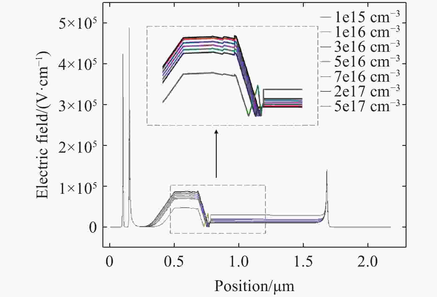
Figure 2. SMUTC-PD’s electric field intensity distribution at different doping concentrations in the electric field regulation layer
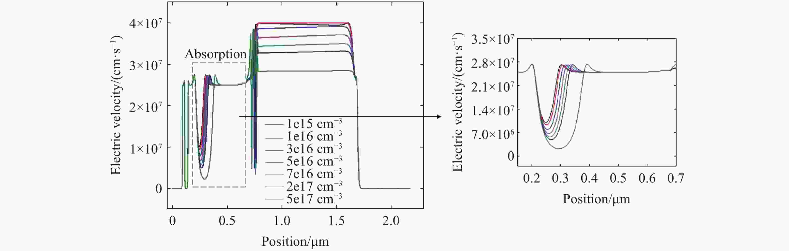
Figure 3. SMUTC-PD’s electron velocity distributions at different doping concentrations in the electric field regulation layer
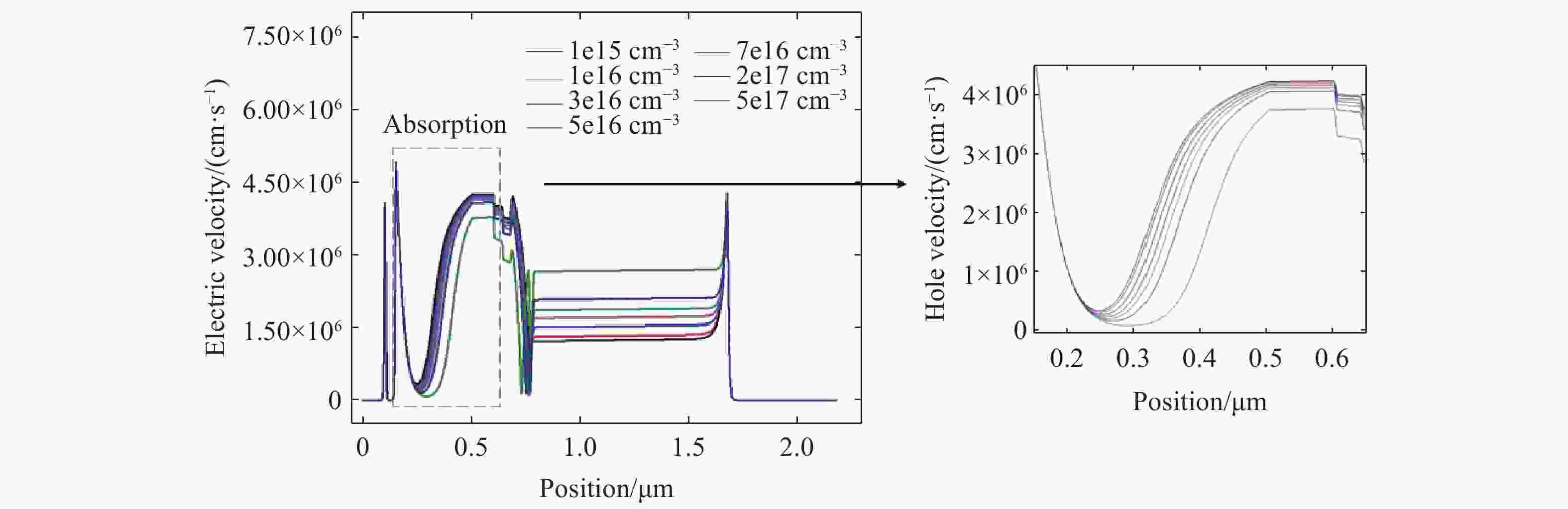
Figure 4. SMUTC-PD’s hole velocity distributions at different doping concentrations in the electric field regulation layer
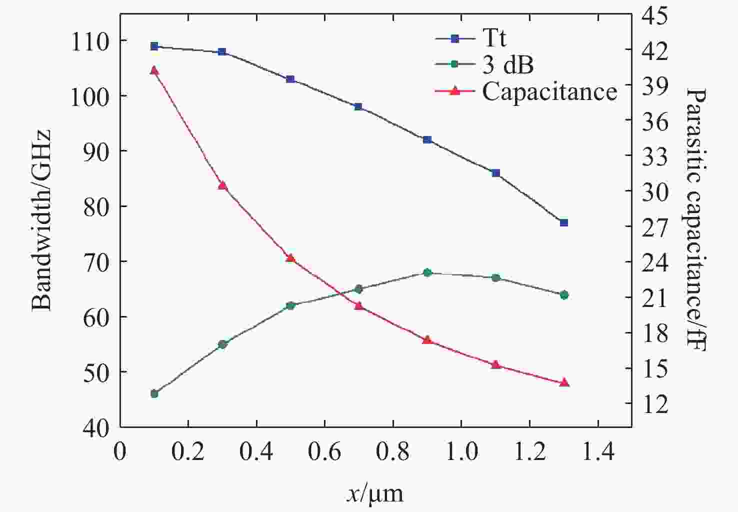
Figure 5. SMUTC-PD’s frequency response and parasitic capacitance with different collector layer thicknesses
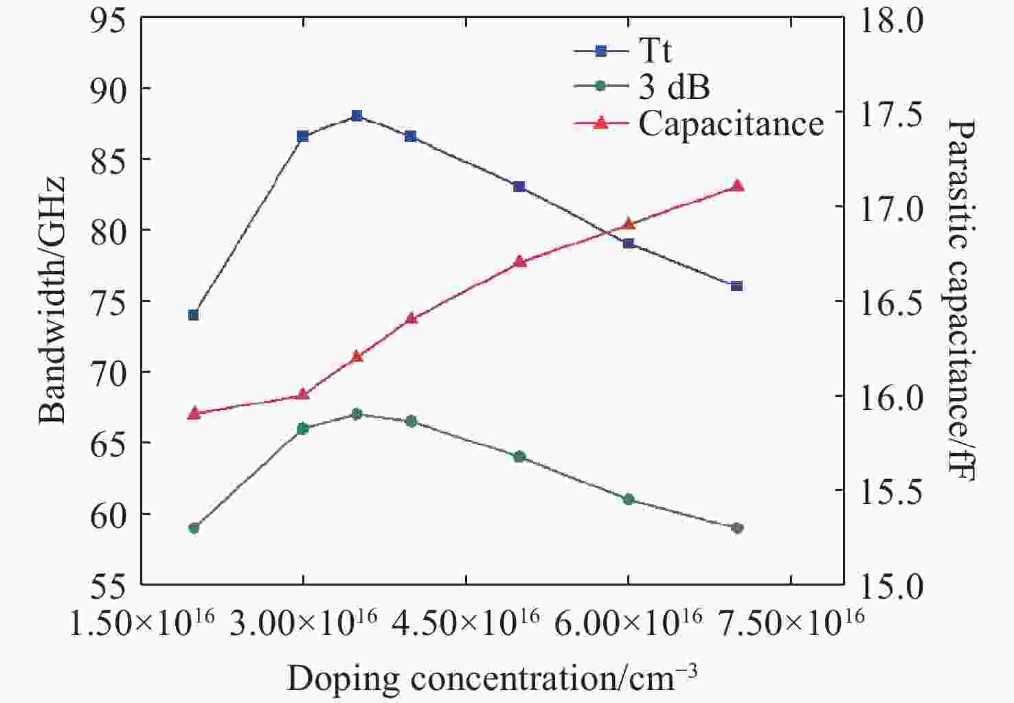
Figure 6. SMUTC-PD’s photo-response bandwidth and parasitic capacitance with different doping concentrations in the p-doped absorption region
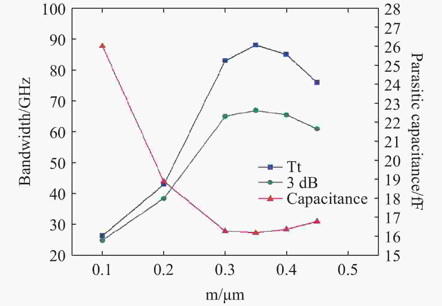
Figure 7. SMUTC-PD’s photo-response bandwidth and parasitic capacitance with different thicknesses of the p-doped absorption region
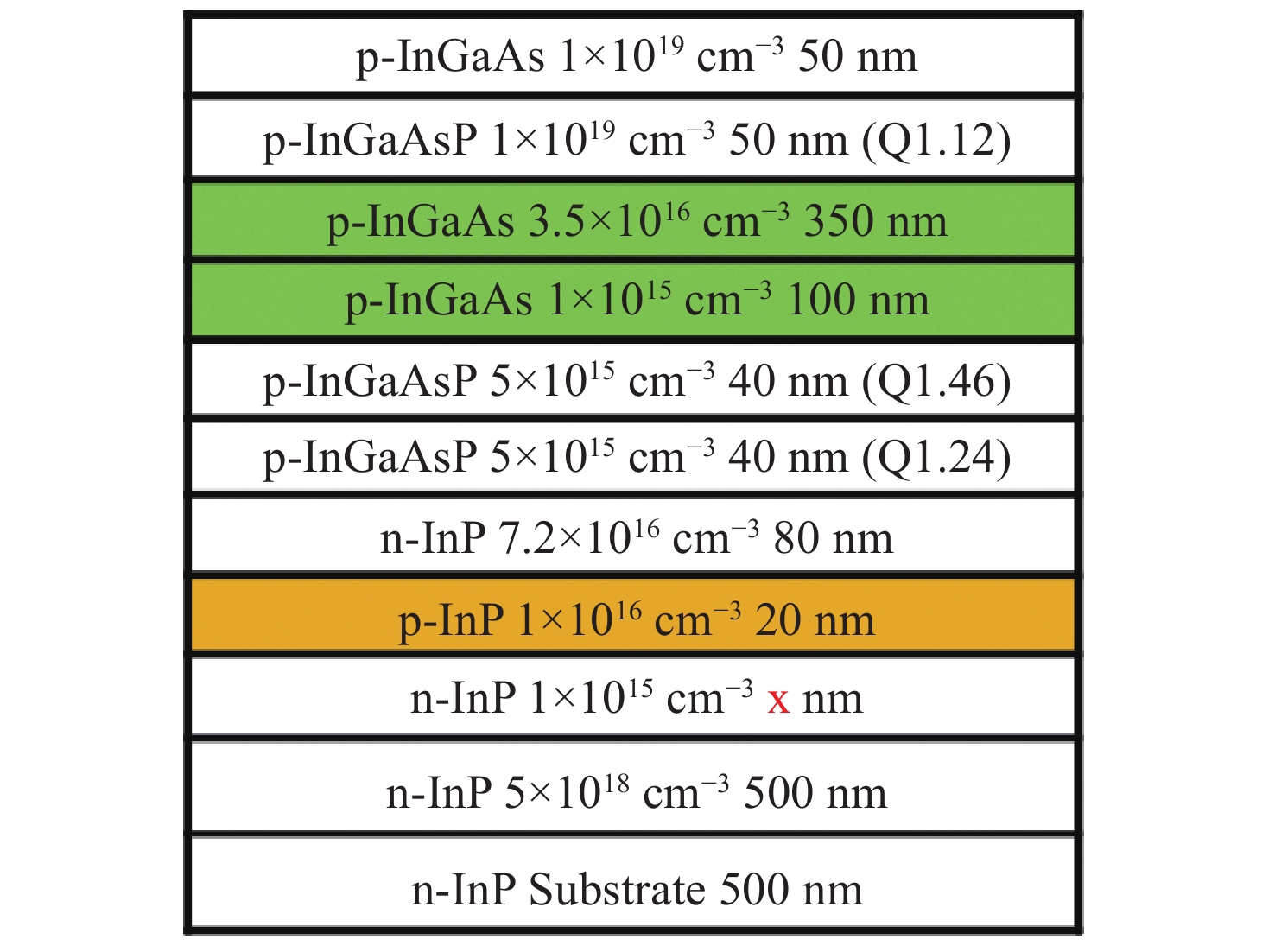
Table 1. Material parameters of the simulation
Parameter InP InGaAs Electron mobility, μn 5400 cm2/Vs12000 cm2/VsHole mobility, μp 200 cm2/Vs 300 cm2/Vs Conduction band density of states, Nc 1.1×1019 cm−3 7.7×1018 cm−3 Valence band density of states, Nv 5.7×1017 cm−3 2.1×1017 cm−3 Electron Saturation velocity 2.6×107 cm/s 2.5×107 cm/s Hole saturation velocity 5×106 cm/s 5×106 cm/s Electron and Hole lifetime 2×10⁻⁹ s 1×10⁻⁷ s Electron Auger coefficient 3.7×10⁻³¹ cm6/s 3.2×10⁻²⁸ cm6/s Hole Auger coefficient 8.7×10⁻³⁰ cm6/s 3.2×10⁻²⁸ cm6/s Real refractive index 3.2 3.51 Imaginary refractive index 0 0.106  下载: 导出CSV
-
[1] PAOLUCCI F, SGAMBELLURI A, EMMERICH R, et al. Openconfig control of 100G/400G filterless metro networks with configurable modulation format and FEC[C]. 2019 Optical Fiber Communications Conference and Exhibition (OFC), IEEE, 2019: 1-3, doi: 10.1364/OFC.2019.Tu3H.4. [2] ZHANG K R, HUANG Y Q, DUAN X F. Design and analysis of hybrid integrated high-speed mushroom vertical PIN photodetector[J]. Applied Mechanics and Materials, 2013, 411-414: 1455-1458. doi: 10.4028/www.scientific.net/AMM.411-414.1455 [3] EFFENBERGER F J, JOSHI A M. Ultrafast, dual-depletion region, InGaAs/InP p-i-n detector[J]. Journal of Lightwave Technology, 1996, 14(8): 1859-1864. doi: 10.1109/50.532024 [4] KATO K, HATA S, KAWANO K, et al. Design of ultrawide-band, high-sensitivity p-i-n photodetectors[J]. IEICE Transactions on Electronics, 1993, E76-C(2): 214-221. [5] LI X, DEMIGUEL S, LI N, et al. Backside illuminated high saturation current partially depleted absorber photodetecters[J]. Electronics Letters, 2003, 39(20): 1466-1467. doi: 10.1049/el:20030927 [6] ISHIBASHI T, ITO H. Uni-traveling-carrier photodiodes[J]. Journal of Applied Physics, 2020, 127(3): 031101. doi: 10.1063/1.5128444 [7] LI Q L, LI K J, FU Y, et al. High-power flip-chip bonded photodiode with 110 GHz bandwidth[J]. Journal of Lightwave Technology, 2016, 34(9): 2139-2144. doi: 10.1109/jlt.2016.2520826 [8] SRIVASTAVA S. Simulation study of InP-based uni-traveling carrier photodiode[D]. Cincinnati: University of Cincinnati, 2003. [9] LI J, XIONG B, LUO Y, et al. Ultrafast dual-drifting layer uni-traveling carrier photodiode with high saturation current[J]. Optics Express, 2016, 24(8): 8420-8428. doi: 10.1364/OE.24.008420 [10] CHAO E F, XIONG B, SUN CH ZH, et al. D-band MUTC photodiodes with flat frequency response[J]. IEEE Journal of Selected Topics in Quantum Electronics, 2022, 28(2): 3802208. doi: 10.1109/JSTQE.2021.3115488 [11] ZHEN ZH, HAO R, XING D, et al. Nearly-ballistic optimization design of high-speed uni-traveling-carrier photodiodes[J]. Chinese Journal of Lasers, 2020, 47(10): 1006003. (in Chinese). doi: 10.3788/CJL202047.1006003 [12] ADACHI S. Physical Properties of III-V Semiconductor Compounds[M]. New York: John Wiley & Sons, 1992. [13] SHRESTHA Y R. Numerical simulation of GaAsSb/InP uni-traveling carrier photodiode[D]. Cincinnati: University of Cincinnati, 2005. [14] ISHIBASHI T, FURUTA T, FUSHIMI H, et al. InP/InGaAs uni-traveling-carrier photodiodes[J]. IEICE Transactions on Electronics, 2000, E83-C(6): 938-949. [15] FRIESE S. Atlas. ti 8 Mac-user manual updated for program version 8.4. ATLAS. ti, Berlin, 2019. (查阅网上资料, 未找到本条文献信息, 请确认) . [16] ZHANG P, ZHANG X P, ZHANG R. Design of broadband and high-output power uni-traveling-carrier photodiodes[J]. Optics Communications, 2016, 365: 194-207. doi: 10.1016/j.optcom.2015.11.075 [17] ZHOU G, RUNGE P. Nonlinearities of high-speed p-i-n photodiodes and MUTC photodiodes[J]. IEEE Transactions on Microwave Theory and Techniques, 2017, 65(6): 2063-2072. doi: 10.1109/TMTT.2016.2645152 [18] DONG X W, LIU K, HUANG Y Q, et al. Design of high-speed UTC-PD with optimization of its electron transit performance and parasitic capacitance[J]. IEEE Photonics Journal, 2023, 15(1): 1-9. doi: 10.1109/JPHOT.2023.3234063 [19] SAKAI K, ISHIMURA E, NAKAJI M, et al. High-current back-illuminated partially depleted-absorber p-i-n photodiode with depleted nonabsorbing region[J]. IEEE Transactions on Microwave Theory and Techniques, 2010, 58(11): 3154-3160. doi: 10.1109/TMTT.2010.2075470 -


 下载:
下载:


计量
- 文章访问数: 85
- HTML全文浏览量: 28
- PDF下载量: 7
- 被引次数: 0
