


785 nm semiconductor laser with shallow etched gratings
doi: 10.37188/CO.EN-2024-0019
-
摘要:
本文提出了一种新型 785 nm 半导体金宝搏188软件怎么用 器件。在 p 侧外延中加入了薄限制层和模式扩展层结构,两者对光栅刻蚀深度的调节有很大影响。p 侧波导层的减薄使得光场偏向 n 侧包层。通过协调限制层的束缚效应,可以调节 P 侧的光限制因子。另一方面,模式扩展层的引入促进了 p 侧限制层上模式的扩展。这两个因素都有助于减少光栅蚀刻深度。与已报道的对称波导外延结构相比,新结构在确保足够反射强度和维持谐振的同时,大大减少了光栅的蚀刻深度。此外,为了提高器件的输出性能,还对新的外延结构进行了优化。在传统外延结构的基础上,增加了能量释放层和电子阻挡层,以提高电子复合效率。改进后的结构虽然增益面积较小,但输出性能却与对称波导相当。
Abstract:A new type of 785 nm semiconductor laser device has been proposed. The thin cladding and mode expansion layer structure incorporated into the epitaxy on the p-side significantly impacts the regulation of grating etching depth. Thinning of the p-side waveguide layer makes the light field bias to the n-side cladding layer. By coordinating the confinement effect of the cladding layer, the light confinement factor on the p-side is regulated. On the other hand, the introduction of a mode expansion layer facilitates the expansion of the mode profile on the p side cladding layer. Both these factors contribute positively to reducing the grating etching depth. Compared to the reported epitaxial structures of symmetric waveguides, the new structure significantly reduces the etching depth of the grating while ensuring adequate reflection intensity and maintaining resonance. Moreover, to improve the output performance of the device, the new epitaxial structure has been optimized. Based on the traditional epitaxial structure, an energy release layer and an electron blocking layer are added to improve the electronic recombination efficiency. This improved structure has an output performance comparable to that of a symmetric waveguide, despite being able to have a smaller gain area.
-
Key words:
- surface grating /
- etching depth /
- epitaxial structure /
- recombination efficiency /
- gain area
-
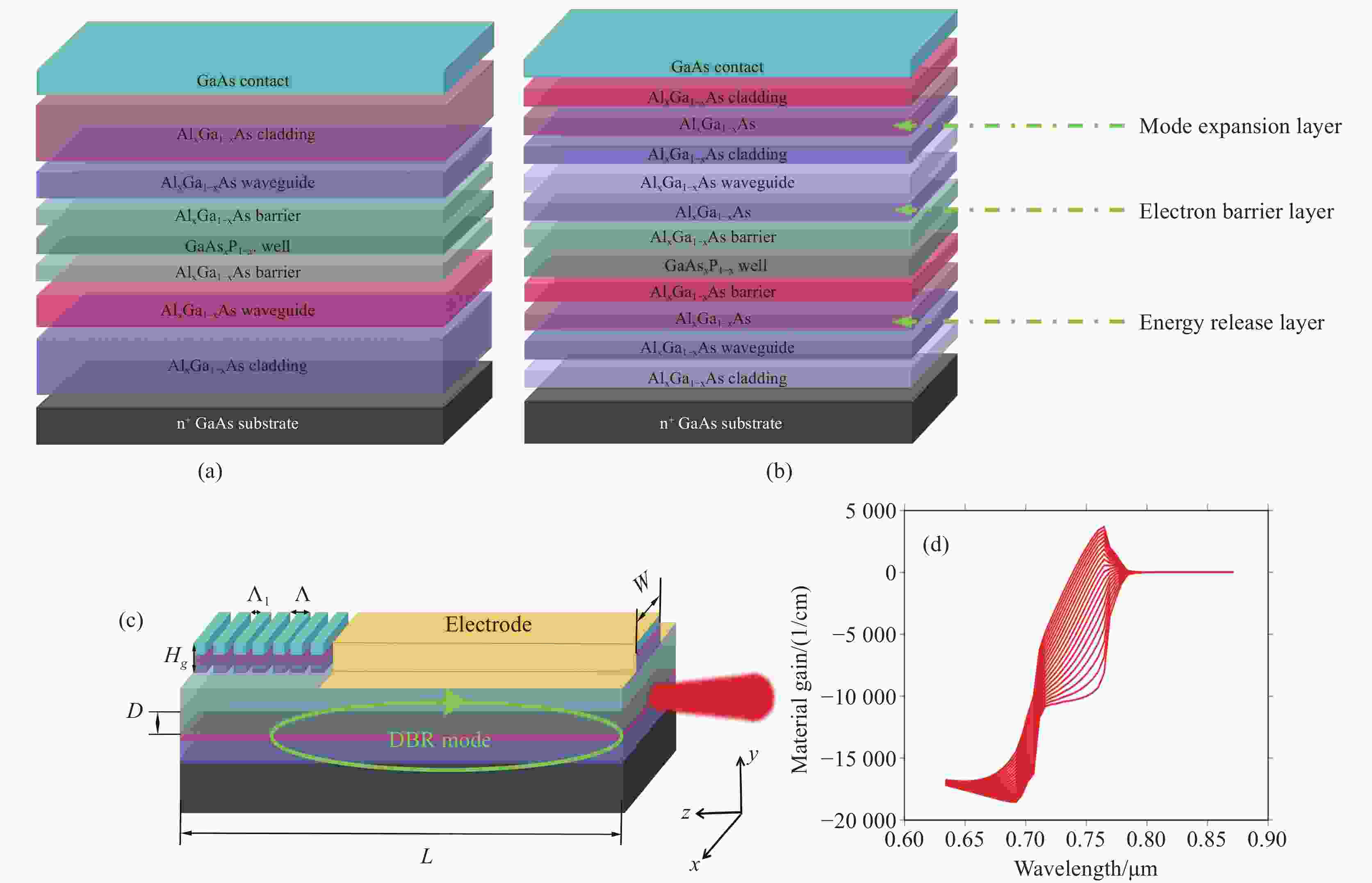
Figure 1. (a) Epitaxial structure of the traditional chip; (b) epitaxial structure of the proposed chip; (c) structure of the DBR laser; (d) gain spectrum
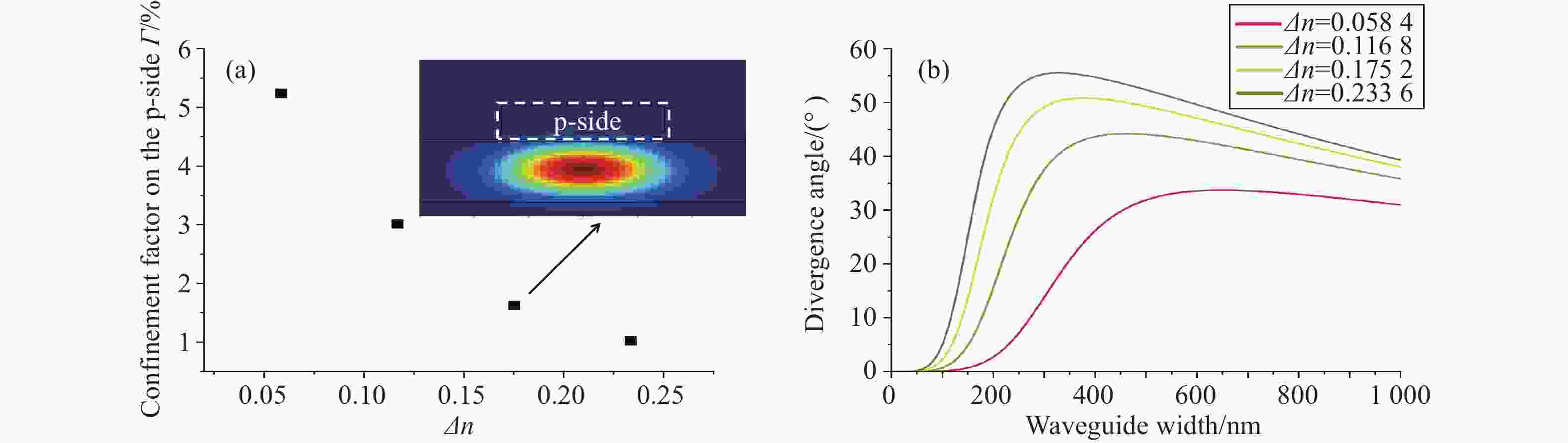
Figure 3. Mode distribution under asymmetric waveguide abtained by FDE. (a)
$ \mathit{\bigtriangleup n} $ versus Γ; (b) waveguide refractive index, waveguide width versus divergence angle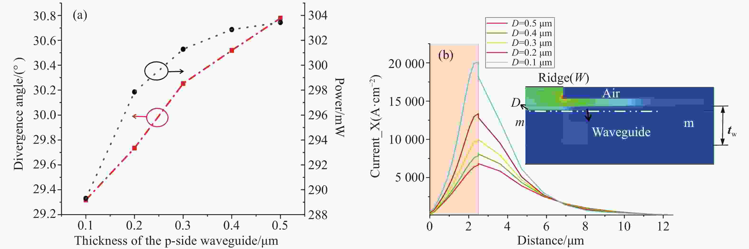
Figure 4. (a) The relationship among different waveguide thicknesses and divergence angle and output power; (b) comparison of current density in the horizontal direction at different etching depths
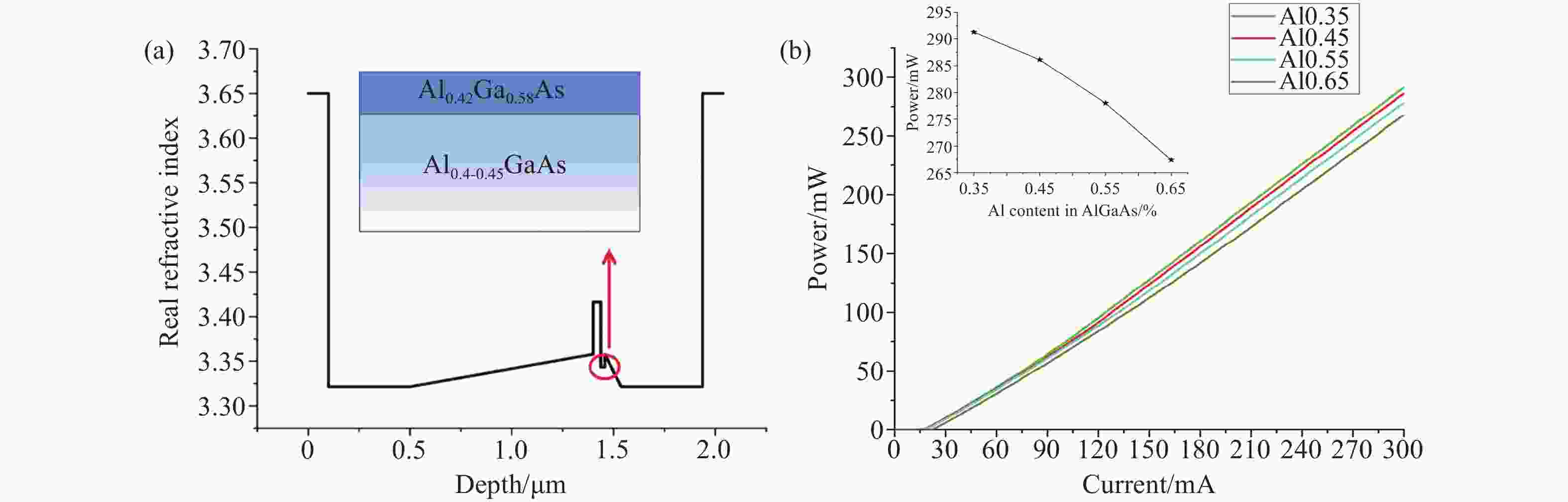
Figure 5. (a) Refractive index of electron-blocking layer; (b) output power at different components on the EBL
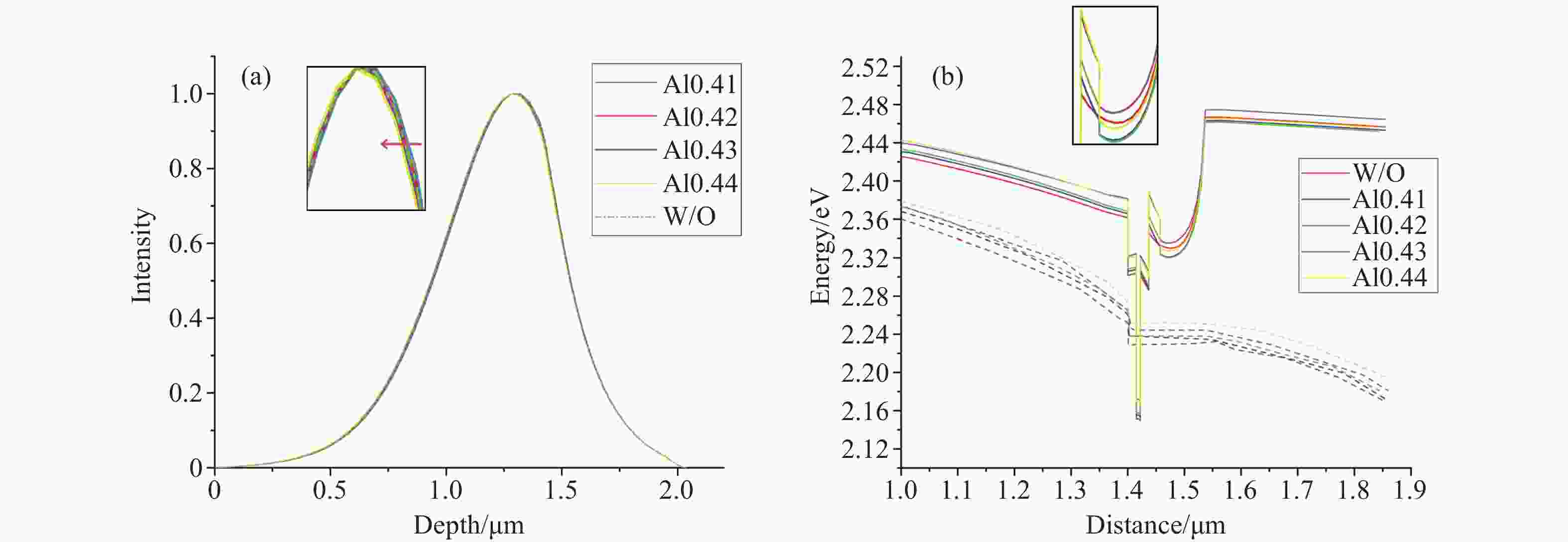
Figure 6. (a) Light field distribution; (b) energy band diagram of different aluminum components
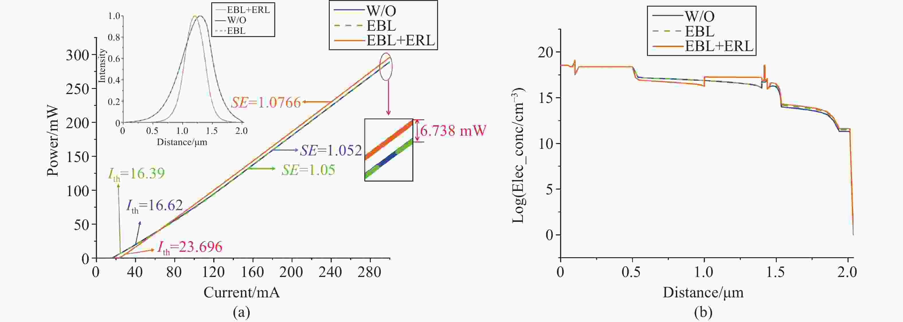
Figure 8. (a) Comparison of output power and (b) electron concentration of different waveguide structures
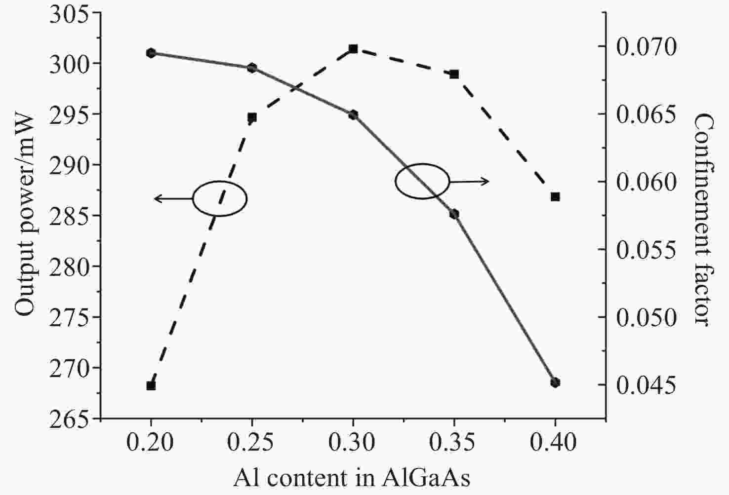
Figure 9. Effect of different Al components of ERL on output power and light confinement factor
Figure 10. Simulated mode distribution for different Al contents. Inset shows their optical confinement factor on p-side and divergence angle
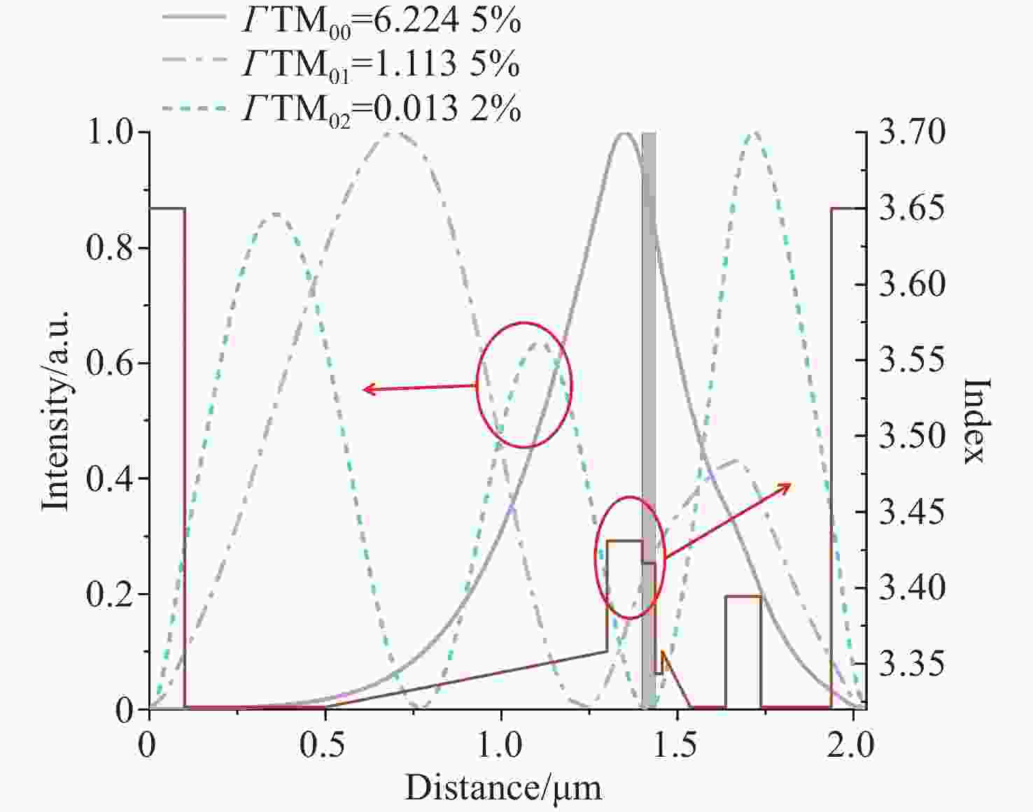
Figure 11. The refractive index and light field distributed in the transverse direction
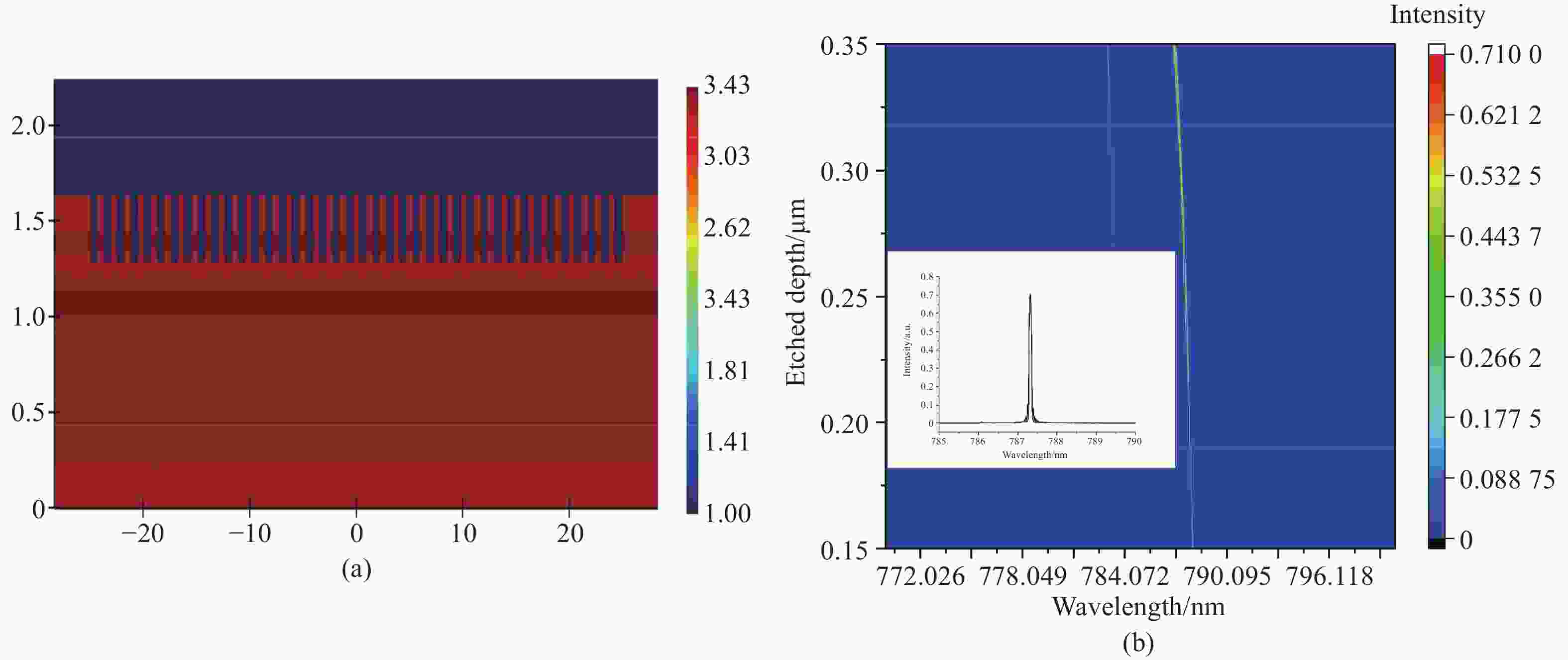
Figure 12. (a) Refractive index distribution of the grating; (b) the relationship between different etching depths and reflectivity
Table 1. Parameters of each layer
Number Layer Material Thickness/μm Doping/m−3 1 Top-cladding Al0.45Ga0.55As 0.2 1×1025 2 Mode expansion Al0.35Ga0.65As 0.1 1×1025 3 Lower-cladding Al0.45Ga0.55As 0.1 1×1025 4 waveguide Al0.45-0.4GaAs 0.08 none 5 Waveguide (EBL) Al0.42Ga0.58As 0.02 none 6 barrier Al0.32Ga0.68As 0.015 none 7 well GaAs0.83P0.17 0.007 none 8 barrier Al0.32Ga0.68As 0.015 none 9 Waveguide (ERL) Al0.3Ga0.7As 0.1 none 10 waveguide Al0.4-0.45GaAs 0.8 none 11 cladding Al0.45Ga0.55As 0.4 1×1025  下载: 导出CSV
-
[1] SUMPF B, KABITZKE J, FRICKE J, et al. Dual-wavelength diode laser with electrically adjustable wavelength distance at 785 nm[J]. Optics Letters, 2016, 41(16): 3694-3697. doi: 10.1364/OL.41.003694 [2] SUMPF B, FRICKE J, MAIWALD M, et al. Wavelength stabilized 785 nm DBR-ridge waveguide lasers with an output power of up to 215 mW[J]. Semiconductor Science and Technology, 2014, 29(4): 045025. doi: 10.1088/0268-1242/29/4/045025 [3] TAN R, QIN Y, HU L Y, et al. Photoelectrochemical sensing based on photocurrent polarity switching strategies[J]. Chinese Journal of Analytical Chemistry,2023,51(5):757-768. [4] LI Z L, XU X R, ZHAN J H, et al. Advanced Materials for Lithography[J]. Chinese Journal of Applied Chemistry, 2023, 40(6): 859-870. [5] LEI Y X, CHEN Y Y, GAO F, et al. 996 nm high-power single-longitudinal-mode tapered gain-coupled distributed feedback laser diodes[J]. Applied Optics, 2019, 58(23): 6426-6432. doi: 10.1364/AO.58.006426 [6] TAN SH Y, ZHAI T, ZHANG R K, et al. Graded doping low internal loss 1060-nm InGaAs/AlGaAs quantum well semiconductor lasers[J]. Chinese Physics B, 2015, 24(6): 064211. doi: 10.1088/1674-1056/24/6/064211 [7] E S Y, ZHOU Y L, ZHANG X, et al. Simulation and experimental research of a high-order Bragg grating semiconductor laser[J]. Applied Optics, 2021, 60(21): 6076-6079. doi: 10.1364/AO.432175 [8] AL-MUHANNA A, ALHARBI A, SALHI A. Waveguide design optimization for long wavelength semiconductor lasers with low threshold current and small beam divergence[J]. Journal of Modern Physics, 2011, 2(4): 225-230. doi: 10.4236/jmp.2011.24031 [9] HOLGUÍN-LERMA J A, NG T K, OOI B S. Narrow-line InGaN/GaN green laser diode with high-order distributed-feedback surface grating[J]. Applied Physics Express, 2019, 12(4): 042007. doi: 10.7567/1882-0786/ab0a57 [10] E S Y, ZHOU Y L, ZHANG X, et al. High-order DBR semiconductor lasers: effect of grating parameters on grating performance[J]. Applied Optics, 2020, 59(28): 8789-8792. doi: 10.1364/AO.402699 [11] ABBASI S P, GOODARZI M, MAHDIEH M H. Optimization of AlGaInAs quantum well in semiconductor lasers[J]. Optical and Quantum Electronics, 2022, 54(8): 517. doi: 10.1007/s11082-022-03914-2 [12] PIKHTIN N A, SLIPCHENKO S O, SOKOLOVA Z N, et al. Internal optical loss in semiconductor lasers[J]. Semiconductors, 2004, 38(3): 360-367. doi: 10.1134/1.1682615 [13] XU Y, JIA L, LIU L, et al. Optical confinement enhancement of AlGaN-based deep-ultraviolet laser diode by using asymmetrically wide waveguide layers[J]. Applied Physics B, 2023, 129(9): 145. doi: 10.1007/s00340-023-08088-7 [14] ERBERT G, BUGGE F, KNAUER A, et al. High-power tensile-strained GaAsP-AlGaAs quantum-well lasers emitting between 715 and 790 nm[J]. IEEE Journal of Selected Topics in Quantum Electronics, 1999, 5(3): 780-784. doi: 10.1109/2944.788451 [15] KAUL T, ERBERT G, MAAßDORF A, et al. Extreme triple asymmetric (ETAS) epitaxial designs for increased efficiency at high powers in 9xx-nm diode lasers[J]. Proceedings of SPIE, 2018, 10514: 105140A. [16] BOTEZ D. Design considerations and analytical approximations for high continuous-wave power, broad-waveguide diode lasers[J]. Applied Physics Letters, 1999, 74(21): 3102-3104. doi: 10.1063/1.124075 [17] AN N, DONG X, SONG Q L, et al. Optimization for designing the waveguide of 980 nm AlGaAs/InGaAs semiconductor laser[J]. Optik, 2015, 126(22): 3477-3481. doi: 10.1016/j.ijleo.2015.07.045 [18] XU B SH, QU K, WANG ZH Y, et al. Investigation of photoelectric performance of laser diode by regulation of p-waveguide layer thickness[J]. Optik, 2020, 200: 163458. doi: 10.1016/j.ijleo.2019.163458 [19] ZUBOV F I, MAXIMOV M V, SHERNYAKOV Y M, et al. Suppression of sublinearity of light–current curve in 850 nm quantum well laser with asymmetric barrier layers[J]. Electronics Letters, 2015, 51(14): 1106-1108. doi: 10.1049/el.2015.1392 [20] YANG J CH, ZHAO D G, JIANG D SH, et al. Performance of InGaN based green laser diodes improved by using an asymmetric InGaN/InGaN multi-quantum well active region[J]. Optics Express, 2017, 25(9): 9595-9602. doi: 10.1364/OE.25.009595 [21] YANG J, ZHAO D G, LIU Z, et al. Suppression the leakage of optical field and carriers in GaN-based laser diodes by using InGaN barrier layers[J]. IEEE Photonics Journal, 2018, 10(4): 1503107. [22] LI X, ZHAO D G, JIANG D SH, et al. Suppression of electron leakage in 808 nm laser diodes with asymmetric waveguide layer[J]. Journal of Semiconductors, 2016, 37(1): 014007. doi: 10.1088/1674-4926/37/1/014007 [23] YANG J, ZHAO D G, ZHU J J, et al. Effect of Mg doping concentration of electron blocking layer on the performance of GaN-based laser diodes[J]. Applied Physics B, 2019, 125(12): 235. doi: 10.1007/s00340-019-7343-4 [24] YANG J CH, ZHAO D G, JIANG D SH, et al. Enhancing the performance of GaN based LDs by using low In content InGaN instead of GaN as lower waveguide layer[J]. Optics & Laser Technology, 2019, 111: 810-813. [25] YANG J J, FAN J, ZOU Y G, et al. Dual-wavelength operation of a tapered laser diode based on a composite DBR grating near 1.03 µm[J]. Optics Letters, 2022, 47(9): 2141-2144. doi: 10.1364/OL.458119 [26] THEURER L S, SUMPF B, MAIWALD M, et al. Ten emitter dual-wavelength Y-branch DBR laser diode array emitting 1 W at 785 nm with a spectral emission width below 60 pm[J]. Journal of Physics Communications, 2021, 5(10): 105017. doi: 10.1088/2399-6528/ac2e55 -


 下载:
下载:


计量
- 文章访问数: 395
- HTML全文浏览量: 261
- PDF下载量: 67
- 被引次数: 0
