


-
摘要: 物质拓扑态的发现是近年来凝聚态物理和材料科学的重大突破。由于存在不同于常规半导体的特殊拓扑量子态(如狄拉克费米子、外尔费米子、马约拉纳费米子等),拓扑量子材料通常能表现出一些新颖的物理特性(如量子反常霍尔效应、三维量子霍尔效应、零带隙的拓扑态、超高的载流子迁移率等),因而在低能耗电子器件和宽光谱光电探测器件领域具有重要的研究价值。本文综述了拓扑量子材料的特性与制备方法以及在光电探测领域的发展现状,重点讨论了拓扑绝缘体与拓扑半金属宽光谱光电探测器的器件结构与性能,同时也对拓扑量子材料在光电探测器领域的发展前景进行了展望。Abstract: The discovery of the topological quantum states of matter is a major milestone in condensed matter physics and material science. Due to the existence of special surface states (e.g. Dirac fermions, Weyl fermions, Majorana fermions), topological quantum materials can usually exhibit some novel physical properties (such as the quantum anomalous Hall effect, 3D quantum Hall effect, Zero-band gap caused by topological states, ultra-high carrier mobility, etc.), which are different from conventional semiconductors. Because of this, there is an abundance of prospects for applications in low-power electronic and optoelectronic devices, especially in broad-spectrum detection. However, the application of topological quantum materials in the field of photoelectric detection is still in the exploratory stage at present. This article reviews the characteristics and preparation methods of topological quantum materials and the development status with respect to optical-sensing materials in photodetectors. The structure and performance of the devices based on topological quantum materials are also mentioned as the development prospects in the field of broad-spectrum detection.
-

图 1 光电探测器类型与探测机理示意图
Figure 1. Photodetector categories and schematic diagram of detection mechanisms
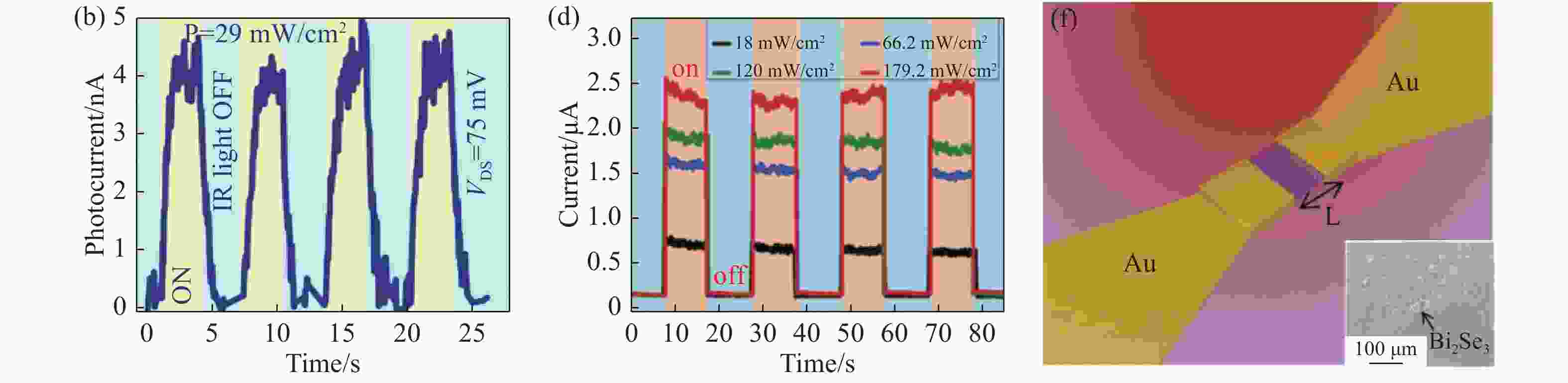
图 3 (a, b) Bi2Se3纳米线光电探测器示意图及其在1064 nm辐射下的光电流响应[60];(c, d) Bi2Se3纳米线/Si异质结结构示意图及其在808 nm下的光电流响应[61];(e)Bi2Se3/Si纳米片器件结构示意图[62];(f)Bi2Se3纳米片太赫兹光电探测器结构示意图[64]
Figure 3. (a, b) Schematic diagram of a Bi2Se3 nanowire photodetector and its photocurrent response under 1064 nm[60]; (c, d) schematic diagram of a Bi2Se3 nanowire/Si heterojunction and its photocurrent response at 808 nm[61]; (e) schematic diagram of a Bi2Se3/Si nanosheet device[62]; (f) schematic diagram of a Bi2Se3 nanosheet terahertz photodetector[64]

图 4 (a-d) Bi2Se3/石墨烯异质结[65]、Bi2Se3/MoO3异质结[66]、Bi2Se3薄膜/钙钛矿量子点[67]及以Bi2Se3薄膜为电极的钙钛矿薄膜光电探测器结构示意图[68]
Figure 4. (a-d) Schematic diagrams of photodetector based on Bi2Se3/graphene[65], Bi2Se3/MoO3 heterojunction[66], Bi2Se3film/ perovskite quantum dots[67] and perovskite film with Bi2Se3 electrodes[68]

图 5 (a, b) Bi2Te3的器件结构示意图及偏振特性[69];(c)Bi2Te3/WS2垂直异质结光电探测器结构示意图[70];(d)以Bi2Te3作为电极的SnS2光电探测器结构示意图[71];(e,f) Bi2Te3/有机小分子平面异质结光电探测器及其能带结构示意图[72]
Figure 5. (a, b) Device structure and polarization characteristics of Bi2Te3[69]; (c, d) schematic diagram of photodetector based on Bi2Te3/WS2 vertical heterojunction[70]and SnS2 with Bi2Te3 electrode[71]; (e, f) schematic diagram of Bi2Te3/organic small molecule planar heterojunction photodetector and its corresponding energy band structure[72]


图 7 (a, b)Sb2Te3薄膜光电探测器及其能带结构示意图[77];(c) Sb2Te3/STO异质结光电探测器阵列示意图[78];(d) Sb2Te3/MoS2异质结光电晶体管示意图[79]
Figure 7. (a, b) Schematic diagram of Sb2Te3 thin film photodetector and its corresponding charge transfer mechanism[77]; (c,d) schematic diagrams of Sb2Te3/STO heterojunction array[78] and Sb2Te3/MoS2 heterojunction phototransistor[79]

图 10 (a, b) Cd3As2薄膜/并五苯异质结能带结构及在不同波段下的光电流响应特性[93];(c, d) Cd3As2薄膜、Cd3As2/DPEPO和Cd3As2/PEDOT:PSS异质结光谱吸收特性及在不同条件下的响应度[94]
Figure 10. (a, b) Charge transfer mechanism and photocurrent response characteristics of Cd3As2 film/Pentacene[93];(c,d)absorption spectra of Cd3As2 film, Cd3As2/DPEPO and Cd3As2/PEDOT:PSS heterojunction and responsivities under different wavebands[94]

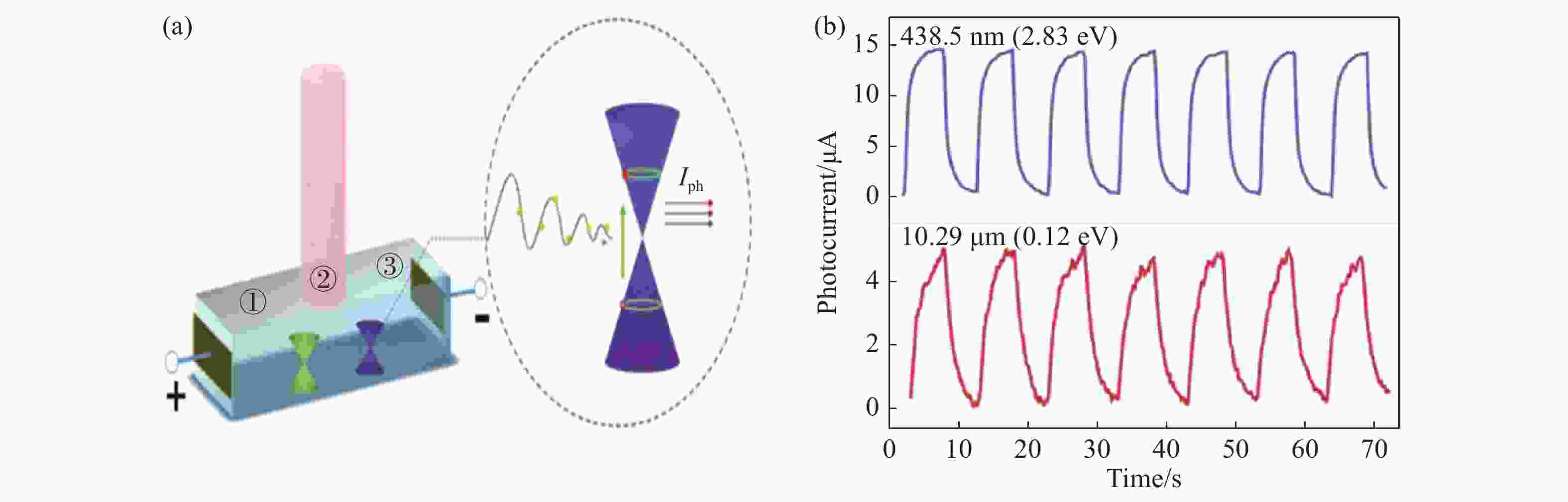


图 14 拓扑量子材料光电探测器的响应率与波长分布
Figure 14. The responsivity and wavelength distributions of topological quantum materials
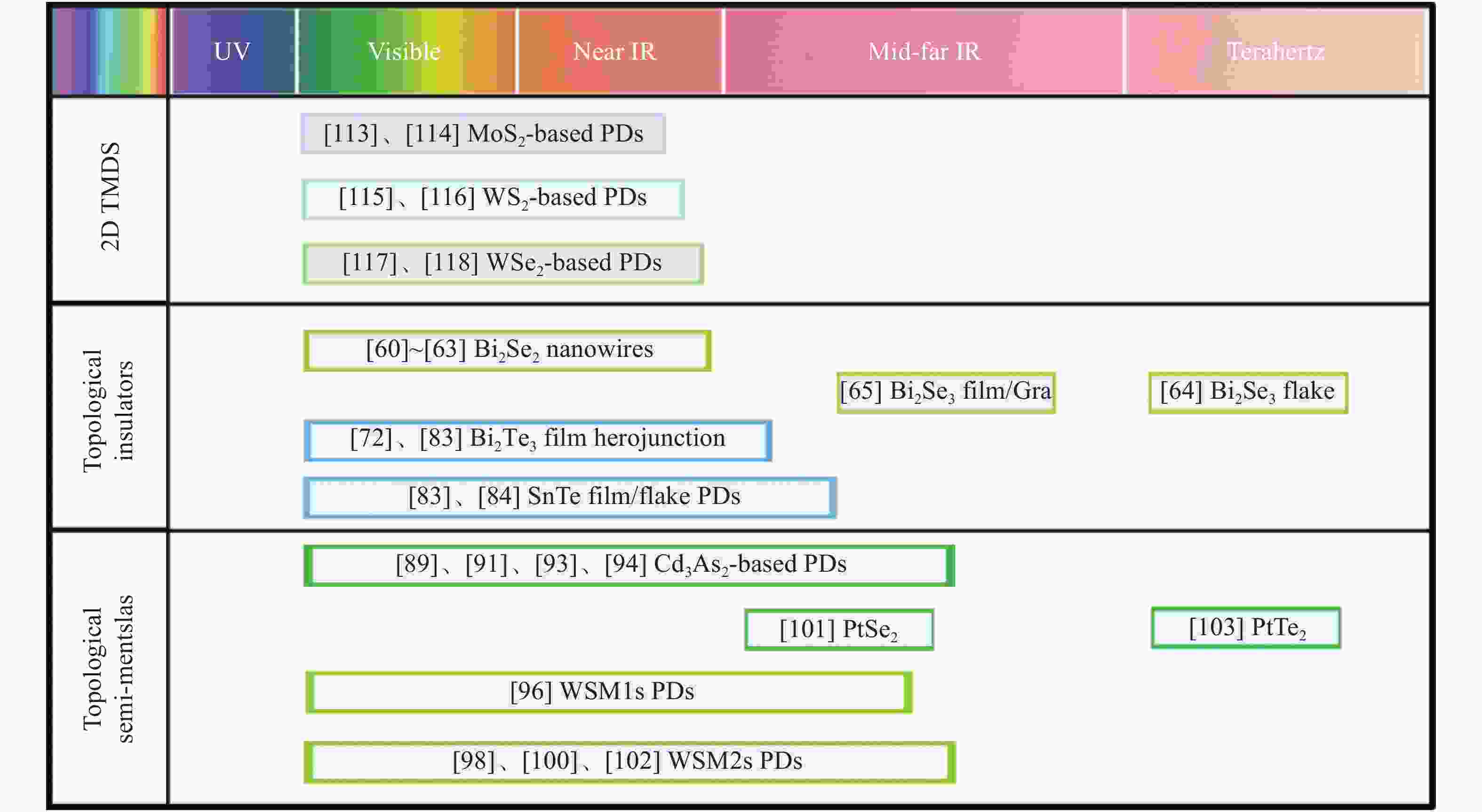
图 15 二维材料与拓扑量子材料光电探测器响应波段对比
Figure 15. Detection ranges of two-dimensional materials and topological quantum materials
表 1 基于拓扑绝缘体的光电探测器性能参数
Table 1. Performance parameters of photodetectors based on topological insulators
Topological Type Active Materials Responsivity (A·W−1) Bias (V) Detectivity (Jones) Response time (ms) Detecting range (nm) Ref. Topological insulator Bi2Se3 NW 300 @1064 nm 0.175 7.5×10⁹ 550/400 532~1064 [60] Bi2Se3 NW/Si 924.2 @808 nm −5 2.38×10¹² 45/47 380~1310 [61] Bi2Se3/Si NW 938.4@890 nm NA 2.35×10¹³ 41/79 Near-infrared [62] Bi2Se3/ln2Se3 1650 @633 nm 5 NA NA Visible [63] Bi2Se3 flakes 75 @THZ 0 2.17×10¹¹ 60 Terahertz [64] Bi2Se3 film/Gra 1.97 @ 3.5 μm 0.5 1.7×10⁹ NA Mid-infrared [65] Bi2Se3film/MoO3 2609 @1310 nm 20 9.43×10¹⁰ 63/78 405~1550 [66] Bi2Te3 film/WS2 30.4 @ 1550 nm 3 2.3×10¹¹ 20/20 375~1550 [70] Bi2Te3/Pentacene 14.89 @650 nm 0 7.8×10¹⁰ 1.89/2.47 450~3500 [72] Bi2Te3/CuPc 23.54 @650 nm 0 1.85×10¹⁰ 1.42/1.98 405~3500 [73] Bi2Te3 flake/Gra 35 @532 nm 1 NA NA 532~1550 [75] WSe2/Bi2Te3 2100@633 nm 1 NA 0.18/0.21 375~1550 [76] Sb2Te3 film 21.7 @980 nm 1 1.22×10¹¹ NA Near-infrared [77] Sb2Te3/STO 0.048 @405 nm 0 8.6×10¹⁰ 0.030/0.095 405~1550 [78] Sb2Te3/MoS2 330 @520 nm −1 1012 0.36/0.47 Visible [79] Topological Crystalline Insulator SnTe film 3.75 @2003 nm 2 NA 310/850 405~3800 [83] SnTe flake 49.03 @650 nm 1 NA 210/730 254~4650 [84] SnTe/Si 2.36 @1064 nm 0 1.54×10¹⁴ 2.2/3.8 Near-infrared [86] SnTe/Bi2Se3 0.146@1550 nm −5 1.15×10¹⁰ 6.9/19.2 Near-infrared [87]  下载: 导出CSV
表 2 基于狄拉克半金属的光电探测器性能参数
Table 2. Performance parameters of photodetectors based on Dirac semi-metal
Topological Type Active materials Responsivity (A·W−1) Bias (V) Detectivity (Jones) Response time (ms) Detecting range (nm) Ref. Dirac semi-metal Cd3As2 0.0059 @633 nm 0.01 NA 6.9 ps(intrinsic) 532~10600 [89] Cd3As2/MoS2 2700 @405 nm 2 NA 0.043/0.065 365~1550 [91] Cd3As2/pentacene 0.0362@650 nm 0.0005 NA 30/60 450~10600 [93] Cd3As2/DPEPO 0.729 @808 nm 0 NA 9.7/11.4 365~10600 [94] Cd3As2/PEDOT:PSS 0.104 @808 nm 0 NA 0.282/0.517 405~10600 [94] Bilayer PtSe2 0.15 @632 nm 0.1 7×10⁸ 1.2 632~10000 [96] PtTe2 1.6 @ THZ 0 NA 0.017/0.16 Terahertz [97] Weyl semi-metal TaAs 0.0007 @438.5 nm 0.0001 1.68×10⁸ NA 438~10290 [98] MoTe2 flake 0.0004 @532 nm 0 1.07×10⁸ 0.043 532~10600 [100] Weyl semi-metal WTe2 flake 250 @3.8 μm (77 K) 0.1 NA NA 514.5~10600 [102] TaIrTe4 0.02@10.6 μm 0 1.8×10⁸ 0.027 532~10600 [103] MoTe2 film/Si 0.19 @980 nm 0 6.8×10¹³ 150/350 (ns) 300~1800 [104] MoTe2 flake/Ge 12460 @915 nm −2 3.3 ×10¹² 5 Near-infrared [105]
下载: 导出CSV
-
[1] ATABAKI A H, MOAZENI S, PAVANELLO F, et al. Integrating photonics with silicon nanoelectronics for the next generation of systems on a chip[J]. Nature, 2018, 556(7701): 349-354. doi: 10.1038/s41586-018-0028-z [2] 王军, 蒋亚东. 室温微测辐射热计太赫兹探测阵列技术研究进展(特邀)[J]. 红外与金宝搏188软件怎么用 工程,2019,48(1):0102001. doi: 10.3788/IRLA201948.0102001WANG J, JIANG Y D. Research development about room temperature terahertz detector array technology with microbolometer structure (invited)[J]. Infrared and Laser Engineering, 2019, 48(1): 0102001. (in Chinese) doi: 10.3788/IRLA201948.0102001 [3] 张猛蛟, 蔡毅, 江峰, 等. 紫外增强硅基成像探测器进展[J]. 中国光学,2019,12(1):19-37. doi: 10.3788/co.20191201.0019ZHANG M J, CAI Y, JIANG F, et al. Silicon-based ultraviolet photodetection: progress and prospects[J]. Chinese Optics, 2019, 12(1): 19-37. (in Chinese) doi: 10.3788/co.20191201.0019 [4] XIA F N, MUELLER T, LIN Y M, et al. Ultrafast graphene photodetector[J]. Nature Nanotechnology, 2009, 4(12): 839-843. doi: 10.1038/nnano.2009.292 [5] 罗曼, 吴峰, 张莉丽, 等. 二维材料偏振响应光电探测[J]. 南通大学学报(自然科学版),2019,18(3):1-10.LUO M, WU F, ZHANG L L, et al. Detection of polarized light using two-dimensional atomic materials[J]. Journal of Nantong University (Natural Science Edition) , 2019, 18(3): 1-10. (in Chinese) [6] 公爽, 田金荣, 李克轩, 等. 新型二维材料在固体金宝搏188软件怎么用 器中的应用研究进展[J]. 中国光学,2018,11(1):18-30. doi: 10.3788/co.20181101.0018GONG SH, TIAN J R, LI K X, et al. Advances in new two-dimensional materials and its application in solid-state lasers[J]. Chinese Optics, 2018, 11(1): 18-30. (in Chinese) doi: 10.3788/co.20181101.0018 [7] WANG F K, ZHANG Y, GAO Y, et al. 2D metal chalcogenides for IR photodetection[J]. Small, 2019, 15(30): 1901347. doi: 10.1002/smll.201901347 [8] BULLOCK J, AMANI M, CHO J, et al. Polarization-resolved black phosphorus/molybdenum disulfide mid-wave infrared photodiodes with high detectivity at room temperature[J]. Nature Photonics, 2018, 12(10): 601-607. doi: 10.1038/s41566-018-0239-8 [9] LI Y F, ZHANG Y T, YU Y, et al. Ultraviolet-to-microwave room-temperature photodetectors based on three-dimensional graphene foams[J]. Photonics Research, 2020, 8(3): 368-374. doi: 10.1364/PRJ.380249 [10] 何珂, 薛其坤. 拓扑量子材料与量子反常霍尔效应[J]. 材料研究学报,2019,29(3):161-177.HE K, XUE Q K. Topological quantum materials and quantum anomalous hall effect[J]. Chinese Journal of Materials Research, 2019, 29(3): 161-177. (in Chinese) [11] 崔亚宁, 任伟. 拓扑量子材料的研究进展[J]. 自然杂志,2019,41(5):348-357.CUI Y N, REN W. Research advances of topological quantum materials[J]. Chinese Journal of Nature, 2019, 41(5): 348-357. (in Chinese) [12] GUI X, PLETIKOSIC I, CAO H B, et al. A new magnetic topological quantum material candidate by design[J]. ACS Central Science, 2019, 5: 900-910. [13] ZHANG T T, JIANG Y, SONG ZH D, et al. Catalogue of topological electronic materials[J]. Nature, 2019, 566(7745): 475-479. doi: 10.1038/s41586-019-0944-6 [14] WANG A Q, YE X G, YU D P, et al. Topological semimetal nanostructures from properties to topotronics[J]. ACS nano, 2020, 14(4): 3755-3778. [15] GAO H, VENDERBOS J W F, KIN Y, et al. Topological semimetals from first principles[J]. Annual Review of Materials Research, 2019, 49: 153-83. doi: 10.1146/annurev-matsci-070218-010049 [16] WANG SH, LIN B C, Wang A Q, et al. Quantum transport in Dirac and Weyl semimetals: a review[J]. Advances in Physics:X, 2017, 2(3): 518-544. doi: 10.1080/23746149.2017.1327329 [17] DAS P K, DI SANTE D, CILENTO F, et al. Electronic properties of candidate type-Ⅱ Weyl semimetal WTe2. a review perspective[J]. Electronic Structure, 2019, 1(1): 014003. doi: 10.1088/2516-1075/ab0835 [18] SCHÜFFELGEN P, SCHMITT T, SCHLEENVOIGT M, et al. Exploiting topological matter for Majorana physics and devices[J]. Solid-State Electronics, 2019, 155: 99-104. doi: 10.1016/j.sse.2019.03.005 [19] YUE Z J, WANG X L, GU M. Topological Insulator Materials for Advanced Optoelectronic Devices[M]. LUO H X. Advanced Topological Insulators. Beverly, MA, USA: Scrivener Publishing LLC, 2019: 45-70. [20] WANG H CH, WANG J. Electron transport in Dirac and Weyl semimetals[J]. Chinese Physics B, 2018, 27(10): 107402. doi: 10.1088/1674-1056/27/10/107402 [21] 张玉平, 唐利斌. 拓扑绝缘体光电探测器研究进展[J]. 红外技术,2020,42(1):1-9.ZHANG Y P, TANG L B. Research progress in photodetectors based on topological insulators[J]. Infrared Technology, 2020, 42(1): 1-9. (in Chinese) [22] CHAN C K, LINDNER N H, REFAEL G, et al. Photocurrents in Weyl semimetals[J]. Physical Review B, 2017, 95(4): 041104. doi: 10.1103/PhysRevB.95.041104 [23] MA J CH, DENG K, ZHENG L, et al. Experimental progress on layered topological semimetals[J]. 2D Materials, 2019, 6(3): 032001. doi: 10.1088/2053-1583/ab0902 [24] ZHE SH, RUI C, KARIM K, et al. Two-dimensional tellurium: progress, challenges, and prospects[J]. Nano-Micro Letters, 2020, 12: 1-34. [25] HAN J Y, WANG J. Photodetectors based on two-dimensional materials and organic thin-film heterojunctions[J]. Chinese Physics B, 2019, 28(1): 017103. doi: 10.1088/1674-1056/28/1/017103 [26] LI Y, SHI ZH F, LI X J, et al. Photodetectors based on inorganic halide perovskites: materials and devices[J]. Chinese Physics B, 2019, 28(1): 017803. doi: 10.1088/1674-1056/28/1/017803 [27] WANG J, HAN J Y, CHEN X Q, et al. Design strategies for two-dimensional material photodetectors to enhance device performance[J]. InfoMat, 2019, 1(1): 33-53. doi: 10.1002/inf2.12004 [28] 胡伟达, 李庆, 陈效双, 等. 具有变革性特征的红外光电探测器[J]. 物理学报,2019,68(12):120701.HU W D, LI Q, CHEN X SH, et al. Recent progress on advanced infrared photodetectors[J]. Acta Physica Sinica, 2019, 68(12): 120701. (in Chinese) [29] FANG Y R, GE Y Q, WANG C, et al. Mid-infrared photonics using 2D materials: status and challenges[J]. Laser &Photonics Reviews, 2020, 14(1): 1900098. [30] CHEN X Q, SHEHZAD K, GAO L, et al. Graphene hybrid structures for integrated and flexible optoelectronics[J]. Advanced Materials, 2020, 32(27): 1902039. [31] ZHANG CH, ZHANG Y, YUAN X, et al. Quantum hall effect based on Weyl orbits in Cd3As2[J]. Nature, 2019, 565(7739): 331-336. doi: 10.1038/s41586-018-0798-3 [32] TANG F D, REN Y F, WANG P P, et al. Three-dimensional quantum hall effect and metal-insulator transition in ZrTe5[J]. Nature, 2019, 569(7757): 537-541. doi: 10.1038/s41586-019-1180-9 [33] VERGNIORY M G, ELCORO L, FELSER C, et al. A complete catalogue of high-quality topological materials[J]. Nature, 2019, 566(7745): 480-485. doi: 10.1038/s41586-019-0954-4 [34] TANG F, PO H C, VISHWANATH A, et al. Comprehensive search for topological materials using symmetry indicators[J]. Nature, 2019, 566(7745): 486-489. doi: 10.1038/s41586-019-0937-5 [35] ZHANG Y, ZHANG F, XU Y G, et al. Epitaxial growth of topological insulators on semiconductors (Bi2Se3/Te@Se) toward high-performance photodetectors[J]. Small Methods, 2019, 3(2): 1900349. [36] BHATTACHARYYA B, GUPTA A, SENGUTTUVAN T D, et al. Topological insulator based dual state photo-switch originating through bulk and surface conduction channels[J]. Physica Status Solidi (B) , 2018, 255(9): 800340. doi: 10.1002/pssb.201800340 [37] CULCER D, KESER A C, LI Y Q, et al. Transport in two-dimensional topological materials: recent developments in experiment and theory[J]. 2D Materials, 2020, 7(2): 022007. doi: 10.1088/2053-1583/ab6ff7 [38] BERNEVIG B A, HUGHES T L, ZHANG SH CH. Quantum spin hall effect and topological phase transition in HgTe quantum wells[J]. Science, 2006, 314(5806): 1757-1761. doi: 10.1126/science.1133734 [39] KÖNIG M, BUHMANN H, MOLENKAMP L W, et al. The quantum spin hall effect: theory and experiment[J]. Journal of the Physical Society of Japan, 2008, 77(3): 031007. doi: 10.1143/JPSJ.77.031007 [40] LIU CH X, HUGHES T L, QI X L, et al. Quantum spin hall effect in inverted type-Ⅱ semiconductors[J]. Physical Review Letters, 2008, 100(23): 236601. doi: 10.1103/PhysRevLett.100.236601 [41] LIU C W, WANG ZH H, QIU R L J, et al. Development of topological insulator and topological crystalline insulator nanostructures[J]. Nanotechnology, 2020, 31(19): 192001. doi: 10.1088/1361-6528/ab6dfc [42] SWATEK P, WU Y, WANG L L, et al.. Gapless Dirac surface states in the antiferromagnetic topological insulator MnBi2Te4[J]. arXiv: 1907.09596, 2019. [43] LI ZH, LI J H, HE K, et al.. Tunable interlayer magnetism and band topology in van der Waals heterostructures of MnBi2Te4-family materials[J]. arXiv: 2003.13485, 2020. [44] FU L. Topological crystalline insulators[J]. Physical Review Letters, 2011, 106(10): 106802. doi: 10.1103/PhysRevLett.106.106802 [45] LI Z, SHAO S, LI N, et al. Single crystalline nanostructures of topological crystalline insulator SnTe with distinct facets and morphologies[J]. Nano Letters, 2013, 13(11): 5443-5448. doi: 10.1021/nl4030193 [46] HSIEH T H, LIN H, LIU J W, et al. Topological crystalline insulators in the SnTe material class[J]. Nature Communications, 2012, 3(1): 982. doi: 10.1038/ncomms1969 [47] SCHOOP L M, DAI X, CAVA R J, et al. Special topic on topological semimetals-new directions[J]. APL Materials, 2020, 8(3): 030401. doi: 10.1063/5.0006015 [48] YAN M ZH, HUANG H Q, ZHANG K N, et al. Lorentz-violating type-Ⅱ Dirac fermions in transition metal dichalcogenide PtTe2[J]. Nature Communications, 2017, 8(1): 257. doi: 10.1038/s41467-017-00280-6 [49] KUSHWAHA S K, KRIZAN J W, FELDMAN B E, et al. Bulk crystal growth and electronic characterization of the 3D Dirac semimetal Na3Bi[J]. APL Materials, 2015, 3(4): 041504. doi: 10.1063/1.4908158 [50] HUANG C, ZHOU B T, ZHANG H Q, et al. Proximity-induced surface superconductivity in Dirac semimetal Cd3As2[J]. Nature Communications, 2019, 10(1): 2217. doi: 10.1038/s41467-019-10233-w [51] GUO J, HUANG Y, WU X SH, et al. Thickness-dependent in-plane thermal conductivity and enhanced thermoelectric performance in p-Type ZrTe5 nanoribbons[J]. Physica Status Solidi (RRL)-Rapid Research Letters, 2019, 13(3): 1800529. doi: 10.1002/pssr.201800529 [52] LV B Q, WENG H M, FU B B, et al. Experimental discovery of Weyl semimetal TaAs[J]. Physical Review X, 2015, 5(3): 031013. doi: 10.1103/PhysRevX.5.031013 [53] SUN Y, WU SH CH, YAN B H. Topological surface states and Fermi arcs of the noncentrosymmetric Weyl semimetals TaAs, TaP, NbAs, and NbP[J]. Physical Review B, 2015, 92(11): 115428. doi: 10.1103/PhysRevB.92.115428 [54] ZHANG CH, NI ZH L, ZHANG J L, et al. Ultrahigh conductivity in Weyl semimetal NbAs nanobelts[J]. Nature Materials, 2019, 18(5): 482-488. doi: 10.1038/s41563-019-0320-9 [55] SOLUYANOV A A, GRESCH D, WANG ZH J, et al. Type-Ⅱ Weyl semimetals[J]. Nature, 2015, 527(7579): 495-498. doi: 10.1038/nature15768 [56] DENG K, WAN G L, DENG P, et al. Experimental observation of topological Fermi arcs in type-Ⅱ Weyl semimetal MoTe2[J]. Nature Physics, 2016, 12(12): 1105-1110. doi: 10.1038/nphys3871 [57] MA J CH, GU Q Q, LIU Y N, et al. Nonlinear photoresponse of type-Ⅱ Weyl semimetals[J]. Nature Materials, 2019, 18(5): 476-481. doi: 10.1038/s41563-019-0296-5 [58] ZHANG X, WANG J, ZHANG SH CH. Topological insulators for high-performance terahertz to infrared applications[J]. Physical Review B, 2010, 82(24): 245107. doi: 10.1103/PhysRevB.82.245107 [59] YAN Y, LIAO ZH M, KE X X, et al. Topological surface state enhanced photothermoelectric effect in Bi2Se3 nanoribbons[J]. Nano Letters, 2014, 14(8): 4389-4394. doi: 10.1021/nl501276e [60] SHARMA A, BHATTACHARYYA B, SRIVASTAVA A K, et al. High performance broadband photodetector using fabricated nanowires of bismuth selenide[J]. Scientific Reports, 2016, 6(1): 19138. doi: 10.1038/srep19138 [61] LIU CH, ZHANG H B, SUN ZH, et al. Topological insulator Bi2Se3 nanowire/Si heterostructure photodetectors with ultrahigh responsivity and broadband response[J]. Journal of Materials Chemistry C, 2016, 4(24): 5648-5655. doi: 10.1039/C6TC01083K [62] DAS B, DAS N S, SARKAR S, et al. Topological insulator Bi2Se3/Si-nanowire-based p-n junction diode for high-performance near-infrared photodetector[J]. ACS Applied Materials &Interfaces, 2017, 9(27): 22788-22798. [63] ZHENG W SH, XIE T, ZHOU Y, et al. Patterning two-dimensional chalcogenide crystals of Bi2Se3 and In2Se3 and efficient photodetectors[J]. Nature Communications, 2015, 6(1): 6972. doi: 10.1038/ncomms7972 [64] TANG W W, POLITANO A, GUO CH, et al. Ultrasensitive room-temperature terahertz direct detection based on a bismuth Selenide topological insulator[J]. Advanced Functional Materials, 2018, 28(31): 1801786. doi: 10.1002/adfm.201801786 [65] KIM J, PARK S, JANG H, et al. Highly sensitive, gate-tunable, room-temperature mid-infrared photodetection based on graphene-Bi2Se3 heterostructure[J]. ACS Photonics, 2017, 4(3): 482-488. doi: 10.1021/acsphotonics.6b00972 [66] YANG M, HAN Q, LIU X CH, et al. Ultrahigh stability 3D TI Bi2Se3/MoO3 thin film Heterojunction infrared Photodetector at optical communication waveband[J]. Advanced Functional Materials, 2020, 30(12): 1909659. doi: 10.1002/adfm.201909659 [67] TANG Y X, JIANG T, ZHOU T, et al. Ultrafast exciton transfer in perovskite CsPbBr3 quantum dots/topological insulator Bi2Se3 film heterostructure[J]. Nanotechnology, 2019, 30(32): 325702. doi: 10.1088/1361-6528/ab166f [68] LIANG F X, LAING L, ZHAO X Y, et al. A sensitive broadband (UV-vis-NIR) perovskite photodetector using topological insulator as electrodes[J]. Advanced Optical Materials, 2019, 7(4): 1801392. [69] YAO J D, SHAO J M, LI S W, et al. Polarization dependent photocurrent in the Bi2Te3 topological insulator film for multifunctional photodetection[J]. Scientific Reports, 2015, 5(1): 14184. doi: 10.1038/srep14184 [70] YAO J D, ZHENG ZH Q, YANG G W. Layered-material WS2/topological insulator Bi2Te3 heterostructure photodetector with ultrahigh responsivity in the range from 370 to 1550 nm[J]. Journal of Materials Chemistry C, 2016, 4(33): 7831-7840. doi: 10.1039/C6TC01453D [71] YAO J D, ZHENG ZH Q, YANG G W. All-layered 2D optoelectronics: a high-performance UV-vis-NIR broadband SnSe Photodetector with Bi2Te3 topological insulator electrodes[J]. Advanced Functional Materials, 2017, 27(33): 1701823. doi: 10.1002/adfm.201701823 [72] YANG M, WANG J, ZHAO Y F, et al. Three-dimensional topological insulator Bi2Te3/Organic thin film heterojunction photodetector with fast and wideband response from 450 to 3500 nanometers[J]. ACS Nano, 2018, 13(1): 755-763. [73] YANG M, WANG J, ZHAO Y F, et al. Polarimetric three-dimensional topological insulators/organics thin film heterojunction photodetectors[J]. ACS Nano, 2019, 13(9): 10810-10817. doi: 10.1021/acsnano.9b05775 [74] SHARMA A, SENGUTTUVAN T D, OJHA V N, et al. Novel synthesis of topological insulator based nanostructures (Bi2Te3) demonstrating high performance photodetection[J]. Scientific Reports, 2019, 9(1): 3804. doi: 10.1038/s41598-019-40394-z [75] QIAO H, YUAN J, XU Z Q, et al. Broadband photodetectors based on graphene-Bi2Te3 heterostructure[J]. ACS Nano, 2015, 9(2): 1886-1894. doi: 10.1021/nn506920z [76] LIU H W, ZHU X L, SUN X X, et al. Self-powered broad-band photodetectors based on vertically stacked WSe2/Bi2Te3p-n heterojunctions[J]. ACS Nano, 2019, 13(11): 13573-13580. doi: 10.1021/acsnano.9b07563 [77] ZHENG K, LUO L B, ZHANG T F, et al. Optoelectronic characteristics of a near infrared light photodetector based on a topological insulator Sb2Te3 film[J]. Journal of Materials Chemistry C, 2015, 3(35): 9154-9160. doi: 10.1039/C5TC01772F [78] SUN H H, JIANG T, ZANG Y Y, et al. Broadband ultrafast photovoltaic detectors based on large-scale topological insulator Sb2Te3/STO heterostructures[J]. Nanoscale, 2017, 9(27): 9325-9332. doi: 10.1039/C7NR01715D [79] LIU H W, LI D, MA CH, et al. Van der Waals epitaxial growth of vertically stacked Sb2Te3/MoS2 p–n heterojunctions for high performance optoelectronics[J]. Nano Energy, 2019, 59: 66-74. doi: 10.1016/j.nanoen.2019.02.032 [80] HUANG S M, HUANG S J, YAN Y J, et al. Extremely high-performance visible light photodetector in the Sb2SeTe2 nanoflake[J]. Scientific Reports, 2017, 7(1): 45413. doi: 10.1038/srep45413 [81] AHER R, BHORDE A, NAIR S, et al. Solvothermal growth of PbBi2Se4 nano-flowers: a material for humidity sensor and photodetector applications[J]. Physica Status Solidi (A) , 2019, 216(11): 1900065. doi: 10.1002/pssa.201900065 [82] SAFDAR M, WANG Q SH, MIRZA M, et al. Topological surface transport properties of single-crystalline SnTe nanowire[J]. Nano Letters, 2013, 13(11): 5344-5349. doi: 10.1021/nl402841x [83] JIANG T, ZANG Y Y, SUN H H. Broadband high-responsivity photodetectors based on large-scale topological crystalline insulator SnTe ultrathin film grown by molecular beam epitaxy[J]. Advanced Optical Materials, 2017, 5(5): 1600727. doi: 10.1002/adom.201600727 [84] YANG J, YU W ZH, PAN ZH H, et al. Ultra-broadband flexible photodetector based on topological crystalline insulator SnTe with high responsivity[J]. Small, 2018, 14(37): 1802598. doi: 10.1002/smll.201802598 [85] GU S H, DING K, PAN J, et al. Self-driven, broadband and ultrafast photovoltaic detectors based on topological crystalline insulator SnTe/Si heterostructures[J]. Journal of Materials Chemistry A, 2017, 5(22): 11171-11178. doi: 10.1039/C7TA02222K [86] ZHANG H B, MAN B Y, ZHANG Q. Topological crystalline insulator SnTe/Si vertical heterostructure photodetectors for high-performance near-infrared detection[J]. ACS Applied Materials &Interfaces, 2017, 9(16): 14067-14077. [87] ZHANG H B, SONG Z L, LI D, et al. Near-infrared photodetection based on topological insulator P-N heterojunction of SnTe/Bi2Se3[J]. Applied Surface Science, 2020, 509: 145290. doi: 10.1016/j.apsusc.2020.145290 [88] CONTE A M, PULCI O, BECHSTEDT F. Electronic and optical properties of topological semimetal Cd3As2[J]. Scientific Reports, 2017, 7(1): 45500. doi: 10.1038/srep45500 [89] WANG Q SH, LI C ZH, GE SH F, et al. Ultrafast broadband photodetectors based on three-dimensional Dirac semimetal Cd3As2[J]. Nano Letters, 2017, 17(2): 834-841. doi: 10.1021/acs.nanolett.6b04084 [90] YAVARISHAD N, HOSSEINI T, KHEIRANDISH E, et al. Room-temperature self-powered energy photodetector based on optically induced Seebeck effect in Cd3As2[J]. Applied Physics Express, 2017, 10(5): 052201. doi: 10.7567/APEX.10.052201 [91] HUANG Z H, JIANG Y D, HAN Q, et al. High responsivity and fast UV-Vis-SWIR photodetector based on Cd3As2/MoS2 heterojunction[J]. Nanotechnology, 2019, 31(6): 064001. [92] WU Y F, ZHANG L, LI C ZH, et al. Dirac semimetal heterostructures: 3D Cd3As2 on 2D Graphene[J]. Advanced Materials, 2018, 30(34): 1707547. doi: 10.1002/adma.201707547 [93] YANG M, WANG J, HAN J Y, et al. Enhanced performance of wideband room temperature photodetector based on Cd3As2 thin film/Pentacene heterojunction[J]. ACS Photonics, 2018, 5(8): 3438-3445. doi: 10.1021/acsphotonics.8b00727 [94] YANG M, WANG J, YANG Y K, et al. Ultraviolet to long-wave infrared photodetectors based on a three- dimensional Dirac semimetal/organic thin film heterojunction[J]. The Journal of Physical Chemistry Letters, 2019, 10(14): 3914-3921. doi: 10.1021/acs.jpclett.9b01619 [95] LÉONARD F, YU W L, COLLINS K C, et al. Strong photothermoelectric response and contact reactivity of the Dirac semimetal ZrTe5[J]. ACS Applied Materials &Interfaces, 2017, 9(42): 37041-37047. [96] YU X CH, YU P, WU D, et al. Atomically thin noble metal dichalcogenide: a broadband mid-infrared semiconductor[J]. Nature Communications, 2018, 9(1): 1545. doi: 10.1038/s41467-018-03935-0 [97] XU H, GUO CH, ZHANG J ZH, et al. PtTe2-based type-Ⅱ dirac semimetal and its van der waals heterostructure for sensitive room temperature terahertz photodetection[J]. Small, 2019, 15(52): 1903362. doi: 10.1002/smll.201903362 [98] CHI SH M, LI ZH L, XIE Y, et al. A wide-range photosensitive Weyl semimetal single crystal-TaAs[J]. Advanced Materials, 2018, 30(43): 1801372-1801379. doi: 10.1002/adma.201801372 [99] OSTERHOUDT G B, DIEBEL L K, GRAY M J, et al. Colossal mid-infrared bulk photovoltaic effect in a type-I Weyl semimetal[J]. Nature Materials, 2019, 18(5): 471-475. doi: 10.1038/s41563-019-0297-4 [100] LAI J W, LIU X, MA J CH, et al. Anisotropic broadband photoresponse of layered type-Ⅱ Weyl semimetal MoTe2[J]. Advanced Materials, 2018, 30(22): 1707152-1707159. doi: 10.1002/adma.201707152 [101] WANG Q SH, ZHENG J CH, HE Y, et al. Robust edge photocurrent response on layered type Ⅱ Weyl semimetal WTe2[J]. Nature Communications, 2019, 10(1): 5736. doi: 10.1038/s41467-019-13713-1 [102] ZHOU W, CHEN J ZH, GAO H, et al. Anomalous and polarization-sensitive photoresponse of Td-WTe2 from visible to infrared light[J]. Advanced Materials, 2019, 31(5): 1804629-1804636. doi: 10.1002/adma.201804629 [103] LAI J W, LIU Y N, MA J CH, et al. Broadband anisotropic photoresponse of the “hydrogen atom” version type-Ⅱ Weyl semimetal candidate TaIrTe[J]. ACS Nano, 2018, 12(4): 4055-4061. doi: 10.1021/acsnano.8b01897 [104] LU ZH J, XU Y, YU Y Q, et al. Ultrahigh speed and broadband few-layer MoTe2/Si 2D-3D heterojunction-based photodiodes fabricated by pulsed laser deposition[J]. Advanced Functional Materials, 2020, 30(9): 1907951. doi: 10.1002/adfm.201907951 [105] CHEN W J, LIANG R R, ZHANG SH Q, et al. Ultrahigh sensitive near-infrared photodetectors based on MoTe2/germanium heterostructure[J]. Nano Research, 2020, 13(1): 127-132. doi: 10.1007/s12274-019-2583-5 [106] YU W ZH, LI SH J, ZHANG Y P, et al. Near-infrared photodetectors based on MoTe2/graphene heterostructure with high responsivity and flexibility[J]. Small, 2017, 13(24): 1700268. doi: 10.1002/smll.201700268 [107] LIU Y J, LIU CH, WANG X M, et al. Photoresponsivity of an all-semimetal heterostructure based on graphene and WTe2[J]. Scientific Reports, 2018, 8(1): 12840. doi: 10.1038/s41598-018-29717-8 [108] LU M Y, CHANG Y T, CHEN H J. Efficient self-driven photodetectors featuring a mixed-dimensional van der waals heterojunction formed from a CdS nanowire and a MoTe2 flake[J]. Small, 2018, 14(40): 1802302. doi: 10.1002/smll.201802302 [109] MAKINO K, KUROMIYA S, TAKANO K, et al. THz pulse detection by multilayered GeTe/Sb2Te3[J]. ACS Applied Materials &Interfaces, 2016, 8(47): 32408-32413. [110] WANG X T, CUI Y, LI T, et al. Recent advances in the functional 2D photonic and optoelectronic devices[J]. Advanced Optical Materials, 2019, 7(3): 1801274. doi: 10.1002/adom.201801274 [111] ROGALSKI A, KOPYTKO M, MARTYNIUK P. Two-dimensional infrared and terahertz detectors: outlook and status[J]. Applied Physics Reviews, 2019, 6(2): 021316. doi: 10.1063/1.5088578 [112] 杨旗, 申钧, 魏兴战, 等. 基于石墨烯的红外探测机理与器件结构研究进展[J]. 红外与金宝搏188软件怎么用 工程,2020,49(1):0103003.YANG Q, SHEN J, WEI X ZH, et al. Recent progress on the mechanism and device structure of graphene-based infrared detectors[J]. Infrared and Laser Engineering, 2020, 49(1): 0103003. (in Chinese) [113] YE L, LI H, CHEN Z F, et al. Near-infrared photodetector based on MoS2/Black phosphorus heterojunction[J]. ACS Photonics, 2016, 3(4): 692-699. doi: 10.1021/acsphotonics.6b00079 [114] HUANG ZH ZH, ZHANG T F, LIU J K, et al. Amorphous MoS2 photodetector with ultra-broadband response[J]. ACS Applied Electronic Materials, 2019, 1(7): 1314-1321. doi: 10.1021/acsaelm.9b00247 [115] ZHU W K, YAN F G, WEI X, et al. Broadband and fast photodetectors based on multilayer p-MoTe2/n-WS2 heterojunction with graphene electrodes[J]. Advanced Materials Letters, 2019, 10(5): 329-333. doi: 10.5185/amlett.2019.2281 [116] TSAI T H, LIANG ZH Y, LIN Y CH, et al. Photogating WS2 photodetectors using embedded WSe2 charge puddles[J]. ACS Nano, 2020, 14(4): 4559-4566. doi: 10.1021/acsnano.0c00098 [117] SUN J CH, WANG Y Y, GUO SH Q, et al. Lateral 2D WSe2 p–n homojunction formed by efficient charge-carrier-type modulation for high-performance optoelectronics[J]. Advanced Materials, 2020, 32(9): 1906499. doi: 10.1002/adma.201906499 [118] ZHENG ZH Q, ZHANG T M, YAO J D, et al. Flexible, transparent and ultra-broadband photodetector based on large-area WSe2 film for wearable devices[J]. Nanotechnology, 2016, 27(22): 225501. doi: 10.1088/0957-4484/27/22/225501 [119] DU Y P, BO X Y, WANG D, et al. Emergence of topological nodal lines and type-Ⅱ Weyl nodes in the strong spin-orbit coupling system InNbX2(X=S, Se)[J]. Physical Review B, 2017, 96(23): 235152. doi: 10.1103/PhysRevB.96.235152 [120] YUAN Y F, WANG W K, ZHOU Y H, et al. Pressure-induced superconductivity in topological semimetal candidate TaTe4[J]. Advanced Electronic Materials, 2020, 6(3): 1901260. doi: 10.1002/aelm.201901260 -

 下载:
下载:


计量
- 文章访问数: 5946
- HTML全文浏览量: 1550
- PDF下载量: 813
- 被引次数: 0
