-
摘要: 经过近10年的发展,超构表面作为一种新型的二维人工微纳结构,在光场特性调控方面展现出了巨大的研究潜力。但要实现小型化、集成化的超构表面光电子器件,还需要进一步发展具备动态调控功能的光学超构表面。本文综述了近年来发展的可形变超构表面的研究进展,简要概述了以纳米剪纸技术为基础的可形变超构表面的设计和实现方法,并重点介绍了其在相位、偏振、光学手性、非线性辐射等方面优异的调控性能及其应用。这种灵活的、易实现的可形变超构表面在光场动态调控方面具有独特优势,为设计和实现新型微纳光电子器件提供了新的策略,有望推动新兴的应变光电子学的发展。Abstract: As one type of novel two-dimensional artificial micro-nano structure, metasurfaces have exhibited strong potential for application in light manipulation in recent decades. However, there is a substantial calling for next-generation optical metasurfaces endowed with remarkable reconfiguration capabilities for practical applications in increasingly miniaturized and integrated opto-electronic devices. In this paper, we review the recent progress of deformable optical metasurfaces mainly fabricated by focused-ion-beam-based nano-kirigami and focus on their excellent performance and applications in the active control of phase, polarization, optical chirality, nonlinear radiation, etc. Deformable metasurfaces with their exceptional flexibility and reconfigurability provide a novel and feasible strategy for the design of functional micro-nano-optoelectronic devices, and immensely promote the development of emerging strainoptronics.
-
Key words:
- metasurfaces /
- nano-kirigami /
- focused ion beam /
- deformable /
- dynamic light manipulation
-
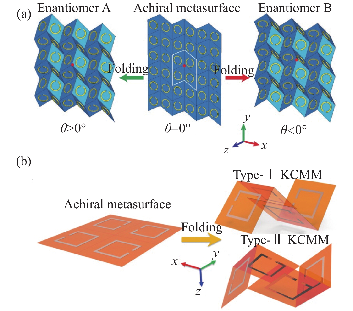
图 1 “三浦折叠”型手性超构材料的结构示意图。(a)通过改变中间二维非手性超构表面的形变方向,可以使两种三维超构材料的手性来回切换[54];(b)基于剪纸形变的手性可调超构材料结构示意图。左边非手性超构表面可折叠成两类手性相反的三维剪纸超构材料[55]
Figure 1. Schematic of the “Miura-ori” chiral metamaterials. (a) By changing the deformed directions of the middle 2D achiral metasurface, the chirality of the two 3D metamaterials can be flexibly switched[54]; (b) schematic of the metamaterials with tunable chirality based on kirigami deformation. The achiral metasurface (left) can be folded into two types of 3D kirigami metamaterials with opposite chirality[55]
图 2 各种不同形貌的三维纳米剪纸/折纸[56-58]。(a), (c), (g)宏观纸质剪纸照片(比例尺:1 cm)及与之对应的(b), (d)~(f), (h)~(j)基于FIB全局辐照得到的三维纳米剪纸结构的SEM图像[56](比例尺:1 μm);(k)三维阿基米德螺旋手性分形剪纸结构的SEM图像[57](比例尺:1 μm);(l)离子辐照剂量增加下具有不同曲率弯曲折纸的SEM图像[58](比例尺:2 μm)
Figure 2. Typical 3D nano-kirigami/origami with various topographies[56-58]. (a), (c), (g) Camera images of the macroscopic paper kirigami (Scale bars: 1 cm) and (b), (d)~(f), (h)~(j) corresponding SEM images of the 3D nano-kirigami with global FIB irradiation[56] (Scale bars: 1 μm); (k) SEM image of the 3D Archimedean spiral chiral fractal kirigami structures[57] (Scale bars: 1 μm); (l) SEM images of an origami structure with different curvatures under an increased ion irradiation dose[58] (Scale bars: 2 μm)
图 3 基于FIB辐照产生应力的微纳加工机理[56, 62]。(a)自支撑纳米金膜在FIB辐照下的残余应力分布和(b)双层应力分布模型[56];(c)固定悬吊结构的一端或两端(用红色方块表示)时,产生两种典型结构变形(向上和向下弯曲)的示意图[56];局域和全局FIB辐照(红色区域)下,悬臂结构的向上刚性折叠(d)和逐步弯曲(e)的SEM图像[62];(f)FIB全局辐照下向下弯曲花瓣型结构的SEM图像[56](比例尺:1 μm)
Figure 3. Micro-nano fabrication mechanism based on FIB-induced stress[56, 62]. (a) Residual stress distribution of a gold nano-film under FIB irradiation and (b) double-layer stress model[56]; (c) schematic of two typical structural deformations (upward and downward bending) when fixing only one or two ends (indicated by the red squares) of the suspended structures[56]; SEM images of (d) the upward rigid folding and (e) gradual bending of suspended cantilevers under local and global FIB irradiations (red areas)[62]; (f) SEM images of a downward bending flower-like structure with global FIB irradiation[56] (Scale bars: 1 μm)
图 4 各种形貌的三维纳米剪纸结构在FIB全局扫描前后的顶视和侧视SEM图像[56, 64]。(a)不同剂量FIB辐照前后的螺旋结构[56];(b)双层螺旋异质结构[56];(c)基于级联FIB刻蚀和Boolean辐照设计四层风车结构的示意图[64];(d)由内层到外层加工的多层四臂风车结构的SEM图像[64](比例尺:1 μm)
Figure 4. Top-view and side-view SEM images of the 3D nano-kirigami with various morphologies before and after global FIB irradiation[56, 64]. (a) A spiral structure before and after FIB irradiation with different doses[56]; (b) a double-layer spiral structure[56]; (c) schematic of a multilayer pinwheel structure designed by cascade FIB milling and Boolean irradiation[64]; (d) SEM images of the multilayer four-arm pinwheel structure fabricated from the innermost layer to outermost layer[64] (Scale bars: 1 μm)
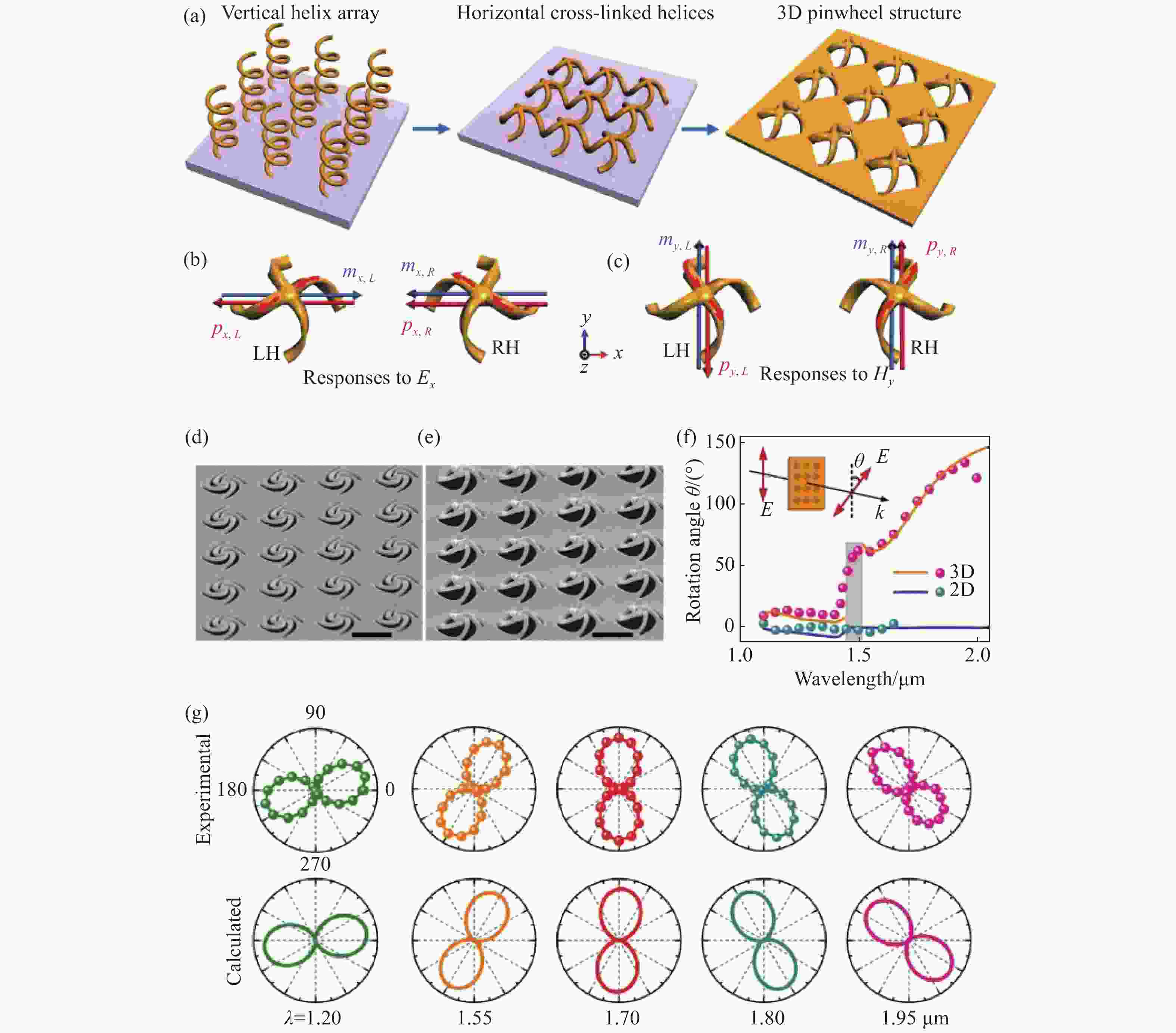
图 5 可形变“闭环”纳米剪纸超构表面的圆双折射特性[56]。(a)从垂直螺旋阵列到三维风车结构的演化过程示意图;(b),(c)LH和RH风车结构分别对入射光电场分量Ex和磁场分量Hy响应的示意图;(d),(e)二维前体和三维风车结构的SEM图像,晶格周期为1.45 μm,三维风车结构高度约为380 nm(比例尺:1 μm);(f)二维和三维LH风车结构在线偏振光入射下,旋转角
$ \theta $ 与入射光波长关系的实验(圆点)和计算(实线)对比;(g)三维风车结构在不同波长处的线偏振旋转极坐标图,上面为实验结果,下面为计算结果。Figure 5. Circular birefringence of deformable “close-loop” nano-kirigami metasurfaces[56]. (a) Schematic of the evolution process from a vertical helix array to a 3D pinwheel structure; (b), (c) schematic of the responses for LH and RH pinwheel structures to the incident E-field component Ex and M-field component Hy; (d), (e) SEM images of the 2D precursor and 3D pinwheel structure, the lattice period is 1.45 μm, and the height of the 3D pinwheel structure is about 380 nm (Scale bars: 1 μm); (f) experimental (circle dots) and calculated (solid lines) rotation angle θ of the 2D and 3D LH pinwheel structures with linear polarized light incidence versus the incident light wavelengths; (g) polar plots of (top) experimental and (bottom) calculated linear polarization rotation angle at specific wavelengths for 3D LH pinwheels
图 6 可形变“闭环”纳米剪纸超构表面的相位调控及衍射偏振转换特性[62]。(a)LH和RH三维风车结构阵列的顶视SEM图像(比例尺:1 μm);(b) LH和RH手性结构的交叉偏振透射相位光谱;(c)计算得到的(左边)LH和RH风车结构在波长1.6 μm处线偏振旋转极坐标图及(右边)LH和RH风车结构线偏振旋转角
$ \theta $ 与入射光波长的关系;(d)由LH和RH手性风车结构交替排布构成的二元线性光栅顶视SEM图像(比例尺:1 μm);(e)线性二元光栅对光场偏振调制示意图;(f)不同入射光波长和探测偏振下的二元线性光栅衍射实验照片,入射光为x偏振Figure 6. Phase and diffractive polarization properties of the deformable “close-loop” nano-kirigami metasurfaces[62]. (a) Top-view SEM image of LH and RH 3D pinwheel structure arrays (Scale bars: 1 μm); (b) cross-polarization transmission phase spectra of the LH and RH chiral structures; (c) (Left) polar plots of the calculated linear polarization rotation angle at 1.6 μm under x-polarized incidence for the LH and RH pinwheels, respectively. (Right) calculated linear polarization rotation angle (
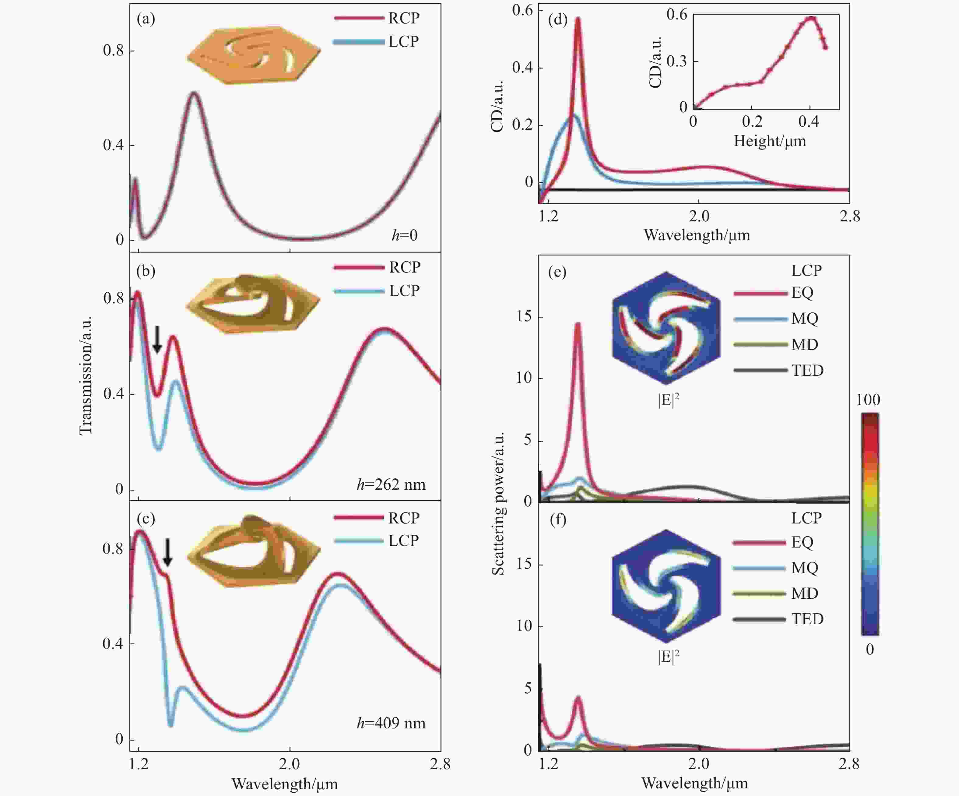
$ \theta $ ) versus wavelength for the LH and RH pinwheels, respectively; (d) top-view SEM image of a linear grating composed of the alternately arranged LH and RH chiral pinwheels (Scale bars: 1 μm); (e) schematic of the polarization control light field with the linear grating; (f) camera images of the linear grating diffraction under different incident wavelengths and detected polarizations. The incident light is x-polarized图 7 可形变超构表面实现圆二色性增强[67]。(a)-(c)LH手性M3超原子在不同形变高度(h=0, 262, 409 nm)下计算的RCP和LCP透射光谱;(d)在(a)(黑线),(b)(蓝线),(c)(红线)中结构所对应的CD谱,其中插图为CD峰强度与M3超原子形变高度的变化关系;(e),(f) (c)中的结构分别在LCP和RCP光入射时的多极矩分量散射强度,插图为超原子表面电场分布的顶视图,超原子的六角晶格间距为s=1.3 μm
Figure 7. Deformable metasurface enabled enhancement of circular dichroism (CD)[67]. (a)-(c) Calculated RCP and LCP transmission spectra of LH chiral M3 meta-atoms at different deformation heights (h=0, 262, 409 nm); (d) CD spectra corresponding to the meta-atoms in (a) (black line), (b) (blue line), (c) (red line). Inset: CD peak intensity versus the height of the M3 meta-atoms; (e), (f) scattering power from various multipole moments induced in the metasurface in (c) under RCP and LCP incidence. Insets: top-view E-field distributions at the surface of the meta-atoms arranged in a hexagonal lattice with a separation of s=1.3 μm
图 8 可形变纳米剪纸超构表面的强非线性圆二色性研究[68]。(a)纳米剪纸超构表面实现非线性圆二色性的示意图,其中RCP基波入射产生的LCP二次谐波(左边)强于LCP基波入射产生的RCP二次谐波(右边);(b),(c)基于FIB加工的纳米剪纸超构表面顶视和侧视SEM图像,C3超原子的六角晶格周期p=1.3 μm(比例尺:1 μm);实验测得的纳米剪纸超构表面的波长依赖二次谐波响应(d)及二次谐波CD谱(e),其中最大CD值位于基波1400 nm处;(f) LCP和RCP单频基波入射下测量的二次谐波谱;(g)在RCPFW-LCPSHG情形下的二次谐波强度依赖关系,其中斜率值2.06体现了一个二阶非线性的光学过程。(f),(g)中的基波波长为1430 nm
Figure 8. Giant nonlinear optical CD of deformable nano-kirigami metasurfaces[68]. (a) Schematic of the nano-kirigami-metasurface-enabled nonlinear CD, in which the LCP SHG waves excited by the incident RCP FW (left) are stronger than the RCP SHG waves excited by the LCP FW incidence (right); (b) top-view and (c) side-view SEM images of the nano-kirigami metasurface using FIB fabrication. The hexagonal lattice period of C3 meta-atoms is p=1.3 μm (Scale bars: 1 μm); (d) measured wavelength-dependent SHG responses of the nano-kirigami metasurface; (e) measured wavelength-dependent SHG-CD, where the maximum CD is at 1400 nm of the FW; (f) measured polarization-resolved SHG spectra under pumping of LCP and RCP FW; (g) power dependence of SHG wave for RCPFW-LCPSHG measurement case. The slope value of 2.06 indicates a second-order nonlinear optical process. The fundamental wavelength in (f) and (g) is 1430 nm
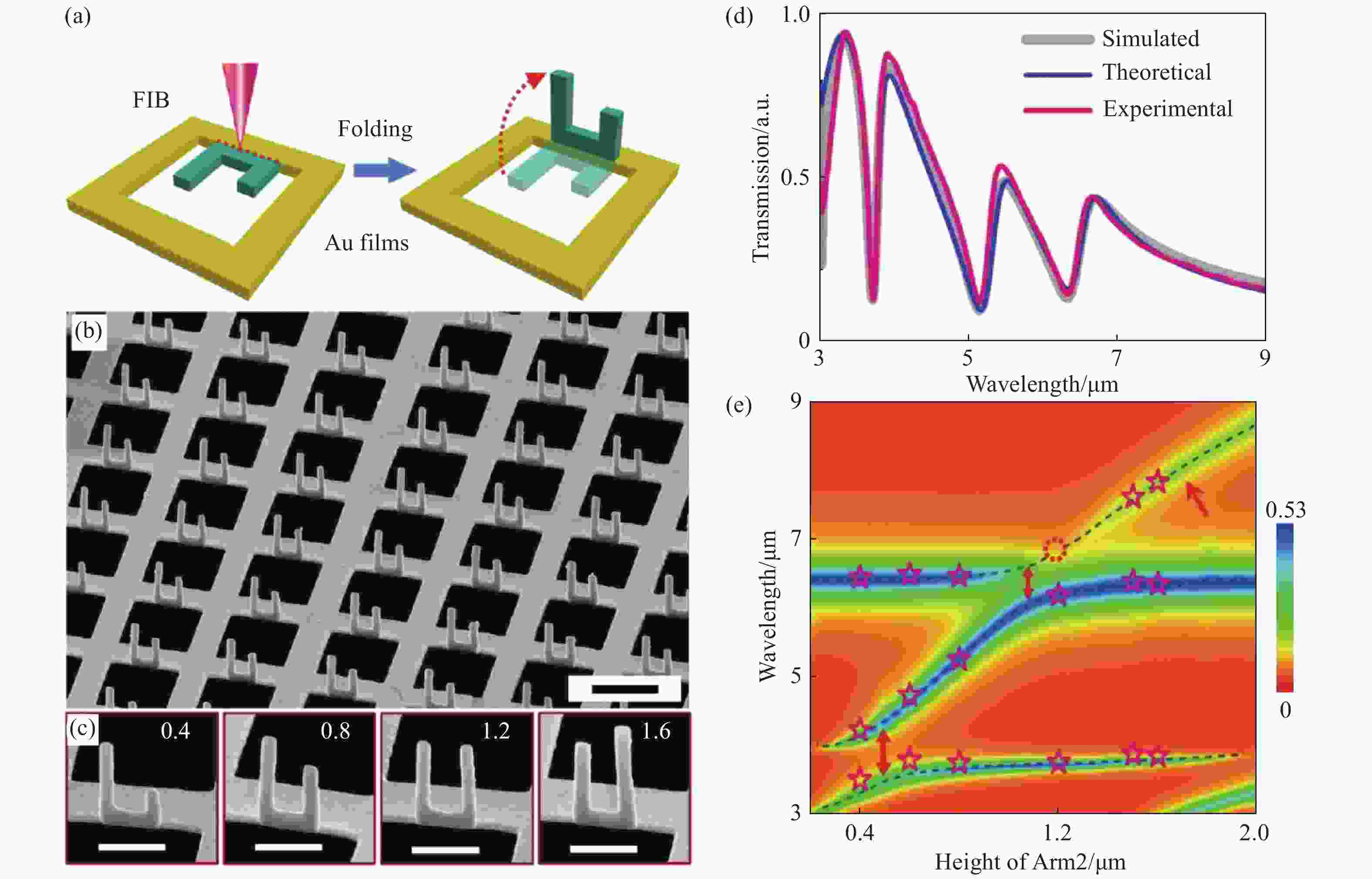
图 9 “树型”纳米剪纸超构表面中Fano共振之间的强耦合研究[69]。(a)基于非对称SRR结构的三维纳米剪纸结构示意图;(b), (c)利用离子束辐照应变折叠制备的三维纳米剪纸SEM图像(比例尺:1 μm);(d)数值模拟、谐振子理论解析以及实验测量的三维纳米剪纸透射光谱,一致显示出三个显著的Fano共振;(e)改变非对称SRR结构一个臂长(保持另一臂长不变)情况下,Fano共振F2产生线性频移。当F2与F1或F3靠近时,Fano共振之间发生显著的反交叉现象,并且反交叉的区域大于相应光谱的线宽,即发生了强耦合。其中彩色光谱为理论模拟得到的系数光谱,星形数据为实验测量得到的Fano共振波长,二者吻合得很好
Figure 9. Strong coupling of Fano resonances in the “tree-type” nano-kirigami metasurfaces[69]. (a) Schematic of 3D nano-kirigami with an asymmetric SRR structure; (b), (c) SEM images of 3D nano-kirigami fabricated by FIB-induced folding (Scale bars: 1 μm); (d) simulated, theoretical, and experimental transmission spectra of the 3D nano-kirigami, consistently showing three significant Fano resonances; (e) color pot of transmission spectra when one arm length of the asymmetric SRR structure is changed (the other arm length is fixed). When F2 is close to F1 or F3, significant anti-crossing phenomenon occurs in Fano resonances, and the anti-crossing area is larger than the line width of the corresponding spectra, that is, strong coupling occurs. The color spectra denote the coefficient spectra obtained by simulations, and the star-shape results plot the Fano resonance wavelengths obtained by experimental measurement, which agree very well
图 10 气动调谐型可重构纳米剪纸超构表面的光场调控研究[74]。(a),(b)可重构Au/SiN双层纳米剪纸超构表面示意图:(a)正方晶格排列的初始二维螺旋阵列以及(b)相应的气压形变三维螺旋阵列;(c),(d)基于FIB加工的初始二维(c)及形变三维(d)螺旋纳米剪纸超构表面侧视SEM图像(比例尺:1 μm);(e)实验测量的二维及三维螺旋纳米剪纸反射光谱(左)以及相应的调制对比度(右);(f)微流体装置照片及(g)螺旋纳米剪纸集成于两个子室间的构造示意图;(h)重复充(
$ \Delta $ P=137 kPa)、放($ \Delta $ P=0 kPa)氮气过程中螺旋纳米剪纸阵列的调制对比度Figure 10. Light manipulation of pneumatically reconfigurable nano-kirigami metasurfaces[74]. (a), (b) Schematic of reconfigurable Au/SiN double-layer nano-kirigami metasurfaces: (a) the initial 2D spiral array arranged in a square lattice and (b) the corresponding pressure-deformed 3D spiral array; (c), (d) side-view SEM images of FIB-based initial 2D (c) and deformed 3D (d) spiral nano-kirigami metasurfaces (Scale bars: 1 μm); (e) measured 2D and 3D spiral nano-kirigami reflection spectra (left) and corresponding modification contrast (right); (f) camera image of the microfluidics device chamber and (g) schematic of the configuration for the nano-kirigami metasurfaces integrated between the connect area of the two sub-chambers; (h) measured reversible modification contrast of spiral nano-kirigami array under repeated inflation (
$ \Delta $ P=137 kPa) and exhaustion ($ \Delta $ P=0 kPa) of nitrogen gas图 11 可形变超构表面在可见光频带的调控应用[64]。(a)具有“环型”Boolean辐照区域的二维风车结构示意图(顶部)及相应的三维形变结构(底部);(b)不同形变高度h三维风车结构的前视图,结构高度变化可诱导入射光的反射相位移动
$ \Delta \phi $ ;(c)11个不同形变高度风车结构的模拟反射相位分布,入射的x偏振平面波λ=633, 532, 473 nm;(d)特定形变应力下风车结构中心平面高度(左)以及相应3个波长对应的反射相移$ \Delta \phi $ (右);(e)3$ \times $ 3风车阵列(h=122 nm, λ=532 nm,$ \Delta \phi $ =${\text{π}}$ )的xy平面(z=2 μm)电场强度分布;(f)单个风车结构(h=122 nm, λ=473, 532, 633 nm)的xz平面(y=0)归一化电场强度分布Figure 11. Visible light manipulation with deformable metasurfaces[64]. (a) Schematic of the 2D pinwheel structure with a “ring-shaped” Boolean irradiation area (top) and the corresponding 3D deformed structure (bottom); (b) front-view of the 3D pinwheels with different deformation heights h. The height change can induce the reflection phase shift
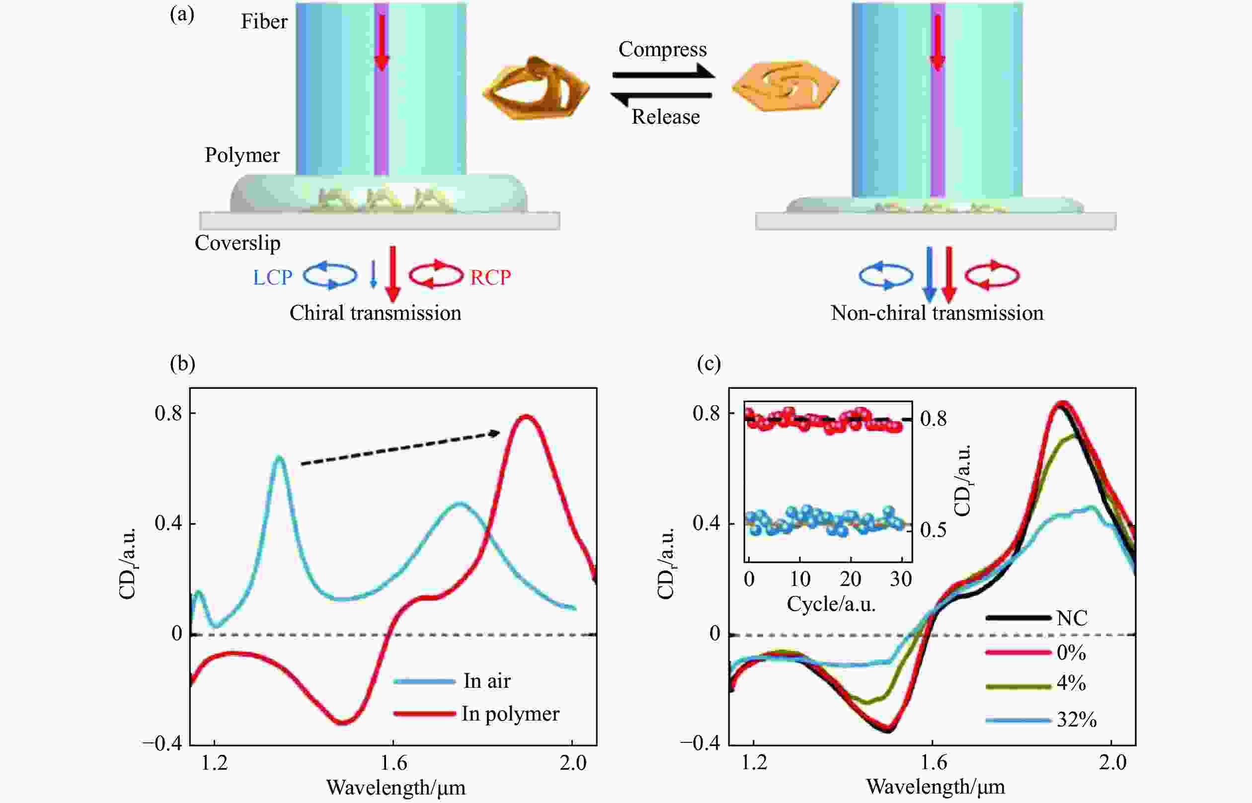
$ \Delta \phi $ of incident light; (c) simulated reflection phase distributions of 11 pinwheels with different deformation heights, the incident x-polarized plane wave with λ=633, 532, 473 nm; (d) the height of the center plane in the pinwheel (left) and the reflection phase shift$ \Delta \phi $ (right) corresponding to the three wavelengths as a function of the deformation stress; (e) E-field intensity distributions of the 3$ \times $ 3 pinwheel array (h=122 nm, λ=532 nm,$ \Delta \phi $ =${\text{π}}$ ) in the xy plane (z=2 μm); (f) normalized E-field intensity distributions of a single pinwheel structure (h=122 nm, λ=473, 532, 633 nm) in the xz plane (y=0)图 12 基于可形变超构表面的圆二色性重构[67]。(a)利用光纤尖端压缩和释放超构表面实现圆二色性可逆调控示意图;(b)实验测量的空气和聚合物中形变超构表面CD谱;(c)实验测量的不同压缩程度形变超构表面CD谱
Figure 12. Reconfigurable CD via deformable metasurfaces[67]. (a) Schematic of reversible modulation of CD by compressing and releasing the metasurface using a fiber tip; (b) measured CD spectra of the deformable metasurfaces in the air and polymer; (c) measured CD spectra of the deformable metasurfaces at different degrees of compression
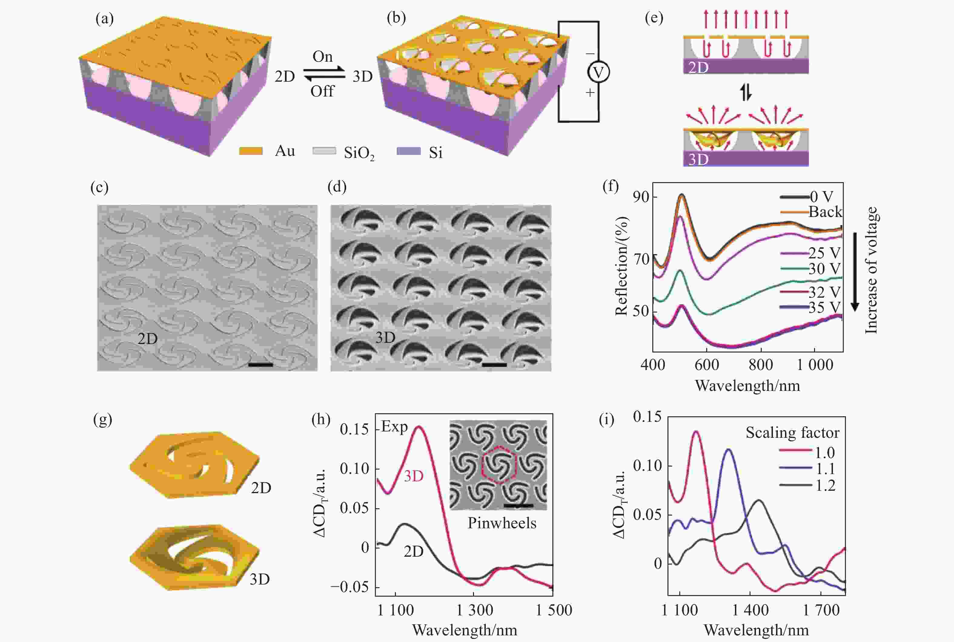
图 13 静电场调谐型可重构纳米剪纸超构表面[75]。(a),(b)二维风车阵列(a)与相应静电力诱导向下形变的三维风车结构(b)可重构示意图;(c),(d)实验加工的二维风车阵列(c)及相应向下形变的三维风车结构(d)侧视SEM图像。施加直流电压V为65 V(比例尺:1 μm);(e)正入射光与二维和三维风车结构的相互作用示意图;(f)不同直流电压下风车结构阵列的反射光谱;(g)单层金膜的二维三臂风车结构及相应形变三维结构示意图;(h)实验测量的初始二维三臂风车结构(V=0)及相应形变三维结构(V=60 V)CD光谱(比例尺:1 μm);(i)实验测量不同比例因子1.0(红线),1.1(蓝线),1.2(黑线)下风车结构二维形变到三维的CD变化谱(
$ \Delta $ CDT=CDT,3D−CDT,2D)Figure 13. Optical chirality of the electrostatic field-based reconfigurable nano-kirigami metasurfaces[75]. (a), (b) Schematic of the 2D pinwheel array (a) and the corresponding electrostatic force-induced downward 3D pinwheel array (b); (c), (d) side-view SEM images of the experimentally fabricated 2D pinwheel array (c) and the corresponding downward 3D pinwheel array (d) when the applied DC voltage V is 65 V (Scale bars: 1 μm); (e) front-view schematic of light scattering under normal incidence for the 2D and 3D pinwheel structures, respectively; (f) reflection spectra of the pinwheel arrays under different DC voltages; (g) schematic of the 2D three-arm pinwheel and the corresponding deformed 3D structure with a single layer of gold film; (h) measured CD spectra of the initial 2D three-arm pinwheels (V=0) and the corresponding deformed 3D structures (V=60 V) (Scale bars: 1 μm); (i) measured changes in CD spectra (
$ \Delta $ CDT=CDT,3D−CDT,2D) from 2D to 3D three-arm pinwheels under scaling factors of 1.0 (red), 1.1 (blue), and 1.2 (black) -
[1] LI S Q, WANG G X, LI X Y, et al. All-dielectric metasurface for complete phase and amplitude control based on Pancharatnam-Berry phase and Fabry-Perot resonance[J]. Applied Physics Express, 2018, 11(10): 105201. doi: 10.7567/APEX.11.105201 [2] OVERVIG A C, SHRESTHA S, MALEK S C, et al. Dielectric metasurfaces for complete and independent control of the optical amplitude and phase[J]. Light:Science &Applications, 2019, 8: 92. [3] BAO L, WU R Y, FU X J, et al. Multi-beam forming and controls by metasurface with phase and amplitude modulations[J]. IEEE Transactions on Antennas and Propagation, 2019, 67(10): 6680-6685. doi: 10.1109/TAP.2019.2925289 [4] BIBBÒ L, LIU Q, KHAN K, et al. High-speed amplitude modulator with a high modulation index based on a plasmonic resonant tunable metasurface[J]. Applied Optics, 2019, 58(10): 2687-2694. doi: 10.1364/AO.58.002687 [5] LEE Y, KIM S J, YUN J G, et al. Electrically tunable multifunctional metasurface for integrating phase and amplitude modulation based on hyperbolic metamaterial substrate[J]. Optics Express, 2018, 26(24): 32063-32073. doi: 10.1364/OE.26.032063 [6] MINATTI G, CAMINITA F, MARTINI E, et al. Synthesis of modulated-metasurface antennas with amplitude, phase, and polarization control[J]. IEEE Transactions on Antennas and Propagation, 2016, 64(9): 3907-3919. doi: 10.1109/TAP.2016.2589969 [7] YANG C, MA Q, BAI G D, et al.. Design of an X-band photoconductive metasurface with variable amplitude control[C]. Proceedings of 2018 International Symposium on Electromagnetic Compatibility (Emc Europe), IEEE, 2018: 990-993. [8] YU N F, GENEVET P, KATS M A, et al. Light propagation with phase discontinuities: generalized laws of reflection and refraction[J]. Science, 2011, 334(6054): 333-337. doi: 10.1126/science.1210713 [9] LIN D M, FAN P Y, HASMAN E, et al. Dielectric gradient metasurface optical elements[J]. Science, 2014, 345(6194): 298-302. doi: 10.1126/science.1253213 [10] KASHEF M M, KASHANI Z G. Multifunctional space-time phase modulated graphene metasurface[J]. Journal of the Optical Society of America B, 2020, 37(11): 3243-3250. doi: 10.1364/JOSAB.401333 [11] ZHOU G N, SUN B H, LIANG Q Y, et al. Beam-deflection short backfire antenna using phase-modulated metasurface[J]. IEEE Transactions on Antennas and Propagation, 2020, 68(1): 546-551. doi: 10.1109/TAP.2019.2934832 [12] ZANG X F, XU W W, GU M, et al. Polarization-insensitive metalens with extended focal depth and longitudinal high-tolerance imaging[J]. Advanced Optical Materials, 2020, 8(2): 1901342. doi: 10.1002/adom.201901342 [13] YU N F, AIETA F, GENEVET P, et al. A broadband, background-free quarter-wave plate based on plasmonic metasurfaces[J]. Nano Letters, 2012, 12(12): 6328-6333. doi: 10.1021/nl303445u [14] LI ZH CH, LIU W W, CHENG H, et al. Realizing broadband and invertible linear-to-circular polarization converter with ultrathin single-layer metasurface[J]. Scientific Reports, 2016, 5: 18106. doi: 10.1038/srep18106 [15] KRUK S, HOPKINS B, KRAVCHENKO I I, et al. Invited article: broadband highly efficient dielectric metadevices for polarization control[J]. APL Photonics, 2016, 1(3): 030801. doi: 10.1063/1.4949007 [16] ZANG X F, DING H ZH, INTARAVANNE Y, et al. A multi-foci metalens with polarization-rotated focal points[J]. Laser &Photonics Reviews, 2019, 13: 1900182. [17] ZANG X F, DONG F L, YUE F Y, et al. Polarization encoded color image embedded in a dielectric metasurface[J]. Advanced Materials, 2018, 30(21): 1707499. doi: 10.1002/adma.201707499 [18] LI G X, ZHANG SH, ZENTGRAF T. Nonlinear photonic metasurfaces[J]. Nature Reviews Materials, 2017, 2(5): 17010. doi: 10.1038/natrevmats.2017.10 [19] LI G X. Geometric phase and nonlinear photonic metasurfaces[J]. Proceedings of SPIE, 2018, 10639: 106390O. [20] ZHANG X Y, LI Q, LIU F F, et al. Controlling angular dispersions in optical metasurfaces[J]. Light:Science &Applications, 2020, 9: 76. [21] KHORASANINEJAD M, AIETA F, KANHAIYA P, et al. Achromatic metasurface lens at telecommunication wavelengths[J]. Nano Letters, 2015, 15(8): 5358-5362. doi: 10.1021/acs.nanolett.5b01727 [22] LI G X. Achromatic metasurface lens at visible wavelengths[J]. Science Bulletin, 2018, 63(6): 333-335. doi: 10.1016/j.scib.2018.02.011 [23] KHORASANINEJAD M, SHI Z, ZHU A Y, et al. Achromatic metalens over 60 nm bandwidth in the visible and metalens with reverse chromatic dispersion[J]. Nano Letters, 2017, 17(3): 1819-1824. doi: 10.1021/acs.nanolett.6b05137 [24] YANG H, LI G H, CAO G T, et al. High efficiency dual-wavelength achromatic metalens via cascaded dielectric metasurfaces[J]. Optical Materials Express, 2018, 8(7): 1940-1950. doi: 10.1364/OME.8.001940 [25] WON R. Achromatic metalens for full-colour imaging[J]. Nature Photonics, 2018, 12(3): 130. doi: 10.1038/s41566-018-0130-7 [26] WANG S M, WU P C, SU V C, et al. A broadband achromatic metalens in the visible[J]. Nature Nanotechnology, 2018, 13(3): 227-232. doi: 10.1038/s41565-017-0052-4 [27] HUANG L L, CHEN X ZH, MÜHLENBERND H, et al. Three-dimensional optical holography using a plasmonic metasurface[J]. Nature Communications, 2013, 4: 2808. doi: 10.1038/ncomms3808 [28] NI X J, KILDISHEV A V, SHALAEV V M. Metasurface holograms for visible light[J]. Nature Communications, 2013, 4: 2807. doi: 10.1038/ncomms3807 [29] HUANG Y W, CHEN W T, TSAI W Y, et al. Aluminum plasmonic multicolor meta-hologram[J]. Nano Letters, 2015, 15(5): 3122-3127. doi: 10.1021/acs.nanolett.5b00184 [30] WANG B, DONG F L, LI Q T, et al. Visible-frequency dielectric metasurfaces for multiwavelength achromatic and highly dispersive holograms[J]. Nano Letters, 2016, 16(8): 5235-5240. doi: 10.1021/acs.nanolett.6b02326 [31] CHEN W T, YANG K Y, WANG C M, et al. High-efficiency broadband meta-hologram with polarization-controlled dual images[J]. Nano Letters, 2014, 14(1): 225-230. doi: 10.1021/nl403811d [32] WEN D D, YUE F Y, LI G X, et al. Helicity multiplexed broadband metasurface holograms[J]. Nature Communications, 2015, 6: 8241. doi: 10.1038/ncomms9241 [33] WANG L, KRUK S, TANG H ZH, et al. Grayscale transparent metasurface holograms[J]. Optica, 2016, 3(12): 1504-1505. doi: 10.1364/OPTICA.3.001504 [34] LESINA A C, RAMUNNO L, BERINI P. Dual-polarization plasmonic metasurface for nonlinear optics[J]. Optics Letters, 2015, 40(12): 2874-2877. doi: 10.1364/OL.40.002874 [35] NOOKALA N, LEE J, TYMCHENKO M, et al. Ultrathin gradient nonlinear metasurface with a giant nonlinear response[J]. Optica, 2016, 3(3): 283-288. doi: 10.1364/OPTICA.3.000283 [36] SEMENIKHINA D V, CHIKOV N I, SEMENIKHIN A I, et al.. Experimental studies of nonlinear metasurface with metamaterial substrate[C]. Proceedings of 2016 24th Telecommunications Forum, IEEE, 2016: 562-565. [37] WAKATSUCHI H, RUSHTON J J, LEE J, et al. Experimental demonstration of nonlinear waveform-dependent metasurface absorber with pulsed signals[J]. Electronics Letters, 2013, 49(24): 1530-1530. doi: 10.1049/el.2013.3010 [38] JOO W J, KYOUNG J, ESFANDYARPOUR M, et al. Metasurface-driven OLED displays beyond 10, 000 pixels per inch[J]. Science, 2020, 370(6515): 459-463. doi: 10.1126/science.abc8530 [39] SAUTTER J, STAUDE I, DECKER M, et al. Active tuning of all-dielectric metasurfaces[J]. ACS Nano, 2015, 9(4): 4308-4315. doi: 10.1021/acsnano.5b00723 [40] DONG K CH, HONG S, DENG Y, et al. A lithography-free and field-programmable photonic metacanvas[J]. Advanced Materials, 2018, 30(5): 1703878. doi: 10.1002/adma.201703878 [41] MIAO Z Q, WU Q, LI X, et al. Widely tunable terahertz phase modulation with gate-controlled graphene metasurfaces[J]. Physical Review X, 2015, 5(4): 041027. doi: 10.1103/PhysRevX.5.041027 [42] THYAGARAJAN K, SOKHOYAN R, ZORNBERG L, et al. Millivolt modulation of plasmonic metasurface optical response via ionic conductance[J]. Advanced Materials, 2017, 29(31): 1701044. doi: 10.1002/adma.201701044 [43] HOWES A, WANG W Y, KRAVCHENKO I, et al. Dynamic transmission control based on all-dielectric Huygens metasurfaces[J]. Optica, 2018, 5(7): 787-792. doi: 10.1364/OPTICA.5.000787 [44] YAO W, TANG L L, WANG J, et al. Spectrally and spatially tunable terahertz metasurface lens based on graphene surface plasmons[J]. IEEE Photonics Journal, 2018, 10(4): 4800909. [45] CAO T, WEI CH W, SIMPSON R E, et al. Rapid phase transition of a phase-change metamaterial perfect absorber[J]. Optical Materials Express, 2013, 3(8): 1101-1110. doi: 10.1364/OME.3.001101 [46] CAO T, WEI CH W, SIMPSON R E, et al. Fast tuning of double Fano resonance using a phase-change metamaterial under low power intensity[J]. Scientific Reports, 2014, 4: 4463. [47] ROY T, ZHANG SH Y, JUNG I W, et al. Dynamic metasurface lens based on MEMS technology[J]. APL Photonics, 2018, 3(2): 021302. doi: 10.1063/1.5018865 [48] SHE A, ZHANG SH Y, SHIAN S, et al. Adaptive metalenses with simultaneous electrical control of focal length, astigmatism, and shift[J]. Science Advances, 2018, 4(2): eaap9957. doi: 10.1126/sciadv.aap9957 [49] ARBABI E, ARBABI A, KAMALI S M, et al. MEMS-tunable dielectric metasurface lens[J]. Nature Communications, 2018, 9: 812. doi: 10.1038/s41467-018-03155-6 [50] GAO H, WANG Y X, FAN X H, et al. Dynamic 3D meta-holography in visible range with large frame number and high frame rate[J]. Science Advances, 2020, 6(28): eaba8595. doi: 10.1126/sciadv.aba8595 [51] LI J X, YU P, ZHANG SH, et al. Electrically-controlled digital metasurface device for light projection displays[J]. Nature Communications, 2020, 11(1): 3574. doi: 10.1038/s41467-020-17390-3 [52] QU G Y, YANG W H, SONG Q H, et al. Reprogrammable meta-hologram for optical encryption[J]. Nature Communications, 2020, 11(1): 5484. doi: 10.1038/s41467-020-19312-9 [53] MAITI R, PATIL C, SAADI M A S R, et al. Strain-engineered high-responsivity MoTe2 photodetector for silicon photonic integrated circuits[J]. Nature Photonics, 2020, 14(9): 578-584. doi: 10.1038/s41566-020-0647-4 [54] WANG Z J, JING L Q, YAO K, et al. Origami-based reconfigurable metamaterials for tunable chirality[J]. Advanced Materials, 2017, 29(27): 1700412. doi: 10.1002/adma.201700412 [55] JING L Q, WANG Z J, ZHENG B, et al. Kirigami metamaterials for reconfigurable toroidal circular dichroism[J]. NPG Asia Materials, 2018, 10(9): 888-898. doi: 10.1038/s41427-018-0082-x [56] LIU ZH G, DU H F, LI J F, et al. Nano-kirigami with giant optical chirality[J]. Science Advances, 2018, 4(7): eaat4436. doi: 10.1126/sciadv.aat4436 [57] TSENG M L, LIN ZH H, KUO H Y, et al. Stress-induced 3D chiral fractal metasurface for enhanced and stabilized broadband near-field optical chirality[J]. Advanced Optical Materials, 2019, 7(15): 1900617. doi: 10.1002/adom.201900617 [58] PAN R H, LI Z C, LIU Z, et al.. Rapid bending origami in micro/nanoscale toward a versatile 3D metasurface[J]. Laser &Photonics Reviews, 2020, 14: 1900179. [59] ARORA W J, SMITH H I, BARBASTATHIS G. Membrane folding by ion implantation induced stress to fabricate three-dimensional nanostructures[J]. Microelectronic Engineering, 2007, 84(5-8): 1454-1458. doi: 10.1016/j.mee.2007.01.182 [60] SAMAYOA M J, HAQUE M A, COHEN P H. Focused ion beam irradiation effects on nanoscale freestanding thin films[J]. Journal of Micromechanics and Microengineering, 2008, 18(9): 095005. doi: 10.1088/0960-1317/18/9/095005 [61] NIX W D, CLEMENS B M. Crystallite coalescence: a mechanism for intrinsic tensile stresses in thin films[J]. Journal of Materials Research, 1999, 14(8): 3467-3473. doi: 10.1557/JMR.1999.0468 [62] LIU ZH G, DU H F, LI ZH Y, et al. Invited article: nano-kirigami metasurfaces by focused-ion-beam induced close-loop transformation[J]. APL Photonics, 2018, 3(10): 100803. doi: 10.1063/1.5043065 [63] LI J F, LIU ZH G. Focused-ion-beam-based nano-kirigami: from art to photonics[J]. Nanophotonics, 2018, 7(10): 1637-1650. doi: 10.1515/nanoph-2018-0117 [64] HAN Y, LIU ZH G, CHEN SH SH, et al. Cascaded multilayer nano-kirigami for extensible 3D nanofabrication and visible light manipulation[J]. Photonics Research, 2020, 8(9): 1506-1511. doi: 10.1364/PRJ.398467 [65] ZHU A Y, CHEN W T, ZAIDI A, et al. Giant intrinsic chiro-optical activity in planar dielectric nanostructures[J]. Light:Science &Applications, 2018, 7: 17158. [66] ZHAO R, ZHANG L, ZHOU J, et al. Conjugated gammadion chiral metamaterial with uniaxial optical activity and negative refractive index[J]. Physical Review B, 2011, 83(3): 035105. doi: 10.1103/PhysRevB.83.035105 [67] LIU ZH G, XU Y, JI CH Y, et al. Fano-enhanced circular dichroism in deformable stereo metasurfaces[J]. Advanced Materials, 2020, 32(8): 1907077. doi: 10.1002/adma.201907077 [68] TANG Y T, LIU ZH G, DENG J H, et al. Nano-kirigami metasurface with giant nonlinear optical circular dichroism[J]. Laser &Photonics Reviews, 2020, 14(7): 2000085. [69] LIU ZH G, LI J F, LIU ZH, et al. Fano resonance Rabi splitting of surface plasmons[J]. Scientific Reports, 2017, 7: 8010. doi: 10.1038/s41598-017-08221-5 [70] CUI A J, LIU Z, LI J F, et al.. Directly patterned substrate-free plasmonic "nanograter'' structures with unusual Fano resonances[J]. Light:Science &Applications, 2015, 4: e308. [71] LIU ZH G, LIU ZH, LI J F, et al. 3D conductive coupling for efficient generation of prominent Fano resonances in metamaterials[J]. Scientific Reports, 2016, 6: 27817. doi: 10.1038/srep27817 [72] TIAN X M, LIU ZH G, LIN H, et al. Five-fold plasmonic Fano resonances with giant bisignate circular dichroism[J]. Nanoscale, 2018, 10(35): 16630-16637. doi: 10.1039/C8NR05277H [73] LIU ZH, DU SH, CUI A J, et al. High-quality-factor mid-infrared toroidal excitation in folded 3D metamaterials[J]. Advanced Materials, 2017, 29(17): 1606298. doi: 10.1002/adma.201606298 [74] CHEN SH SH, WEI W, LIU ZH G, et al. Reconfigurable nano-kirigami metasurfaces by pneumatic pressure[J]. Photonics Research, 2020, 8(7): 1177-1182. doi: 10.1364/PRJ.393333 [75] CHEN SH SH, LIU ZH G, DU H F, et al. Electromechanically reconfigurable optical nano-kirigami[J]. Nature Communications, 2021, 12: 1299. doi: 10.1038/s41467-021-21565-x -


 下载:
下载:


