


-
摘要: 超构表面是由精心设计和排布的亚波长纳米单元组成的平面元件,其可以在微观尺度下调制电磁场,从而实现波前的任意调控。目前,它已被用来灵活地操纵相位、偏振、振幅等各种光学参数。超构透镜是超构表面中相当重要且非常活跃的一个研究方向,由于其厚度在波长量级,与传统光学透镜相比,能够显著增加光学器件的集成度并且降低结构复杂度。但是,单元结构材料的固有色散以及结构几何形状衍射效应导致的色差会严重影响超构透镜的成像质量,从而限制了其在光电子器件中的潜在应用。本文首先讨论超构透镜控制色差的原理。随后回顾了几种重要的成像应用,包括分立波长消色差,宽带聚焦成像,光场成像等重要的成像系统。最后,本文对超构透镜未来的发展方向和应用前景做出展望。Abstract: Metasurface consists of the arrangement of the specially designed subwavelength nano units, which is the two-dimensional counterpart of metamaterial. Metasurface can modulate the electromagnetic field on a microscopic scale to allow the arbitrary wavefront manipulation. At present, it has been used to flexibly control various optical parameters such as phase, polarization, and amplitude. Among all of the applications based on metasurfaces, metalens is no doubt one of the most important and basic research interset. Because its thickness is on the order of wavelength, compared with traditional optical lenses, it can significantly increase the integration of optical devices and reduce the systematic complexity. However, the chromatic aberration caused by the inherent dispersion of the material of the unit structure and the diffraction effect of the structural geometry will severely influence the imaging quality of the metalens, and hence isolating us from a rich variety of advanced applications. Herein, we firstly discuss the principle of controlling chromatic aberration with metalens. Then we review several important imaging applications, including discrete wavelength achromatic, broadband focus imaging, light field imaging and other important imaging systems. Finally, this article makes some prospects for the incoming development direction and potential applications of metalens.
-
Key words:
- metasurface /
- metalens /
- achromatic /
- chromatic aberration control
-

图 1 分立波长消色差超构透镜。(a) 基于三种不同金属微纳颗粒构成的垂直堆叠超构透镜[69];(b) 由三个分割拼接的复合超构透镜实现三个分立波长的消色差[70];(c) 对偏振不敏感的超构透镜,由多扇区透镜(上图)和交错透镜(下图)中的纳米柱组成[71];(d) 具有双折射椭圆柱超构单元的双波长超构透镜[72];(e) 基于偏振操作的具有双波长超构透镜的双光子显微镜[73];(f) 基于超构表面的菲涅尔波带片[74]
Figure 1. Multiwavelength achromatic metalenses. (a) A vertically stacked metalens based on three different metal nano particles[69]; (b) the achromatic effect of three discrete wavelengths is realized by three segmented composite metalens[70]; (c) a polarization-insensitive metalens is composed of nanoposts in multisector lens (above) and interleaved lens (below)[71]; (d) a dual wavelength metalens with birefringent elliptical cylinder meta-atoms[72]; (e) a two-photon microscope with dual-wavelength metalens based on polarization operation[73]; (f) Fresnel zone plate based on metasurface[74]

图 2 算法优化分立波长消色差超构透镜。(a)三波长复消色差衍射透镜[75];(b)基于亚波长等离子体微纳粒子的多波长消色差超构透镜[76];(c)利用全息术原理调控双波长的光场[77]
Figure 2. Algorithm optimization of multiwavelength achromatic metalens. (a) Three-wavelength apochromatic diffractive lens[75]; (b) multiwavelength achromatic metalens based on subwavelength plasma nano particles[76]; (c) the light field which uses the principle of holography to control dual-wavelength[77]

图 3 窄带消色差超构透镜。(a)应用了由二氧化钛纳米柱,电介质薄层和金属背反射器制成的超构单元,以实现具有60 nm以上连续带宽的消色差超构透镜[78];(b)能够实现正,零和超负色散的超构表面设计[79]
Figure 3. Narrowband achromatic metalens. (a) Meta-atoms made of titanium dioxide nano-pillars, a dielectric layer and a metal back reflector which is applied to realize an achromatic metalens with continuous bandwidth above 60 nm[78]; (b) a metasurface design capable of realizing positive, zero and super-negative dispersion[79]
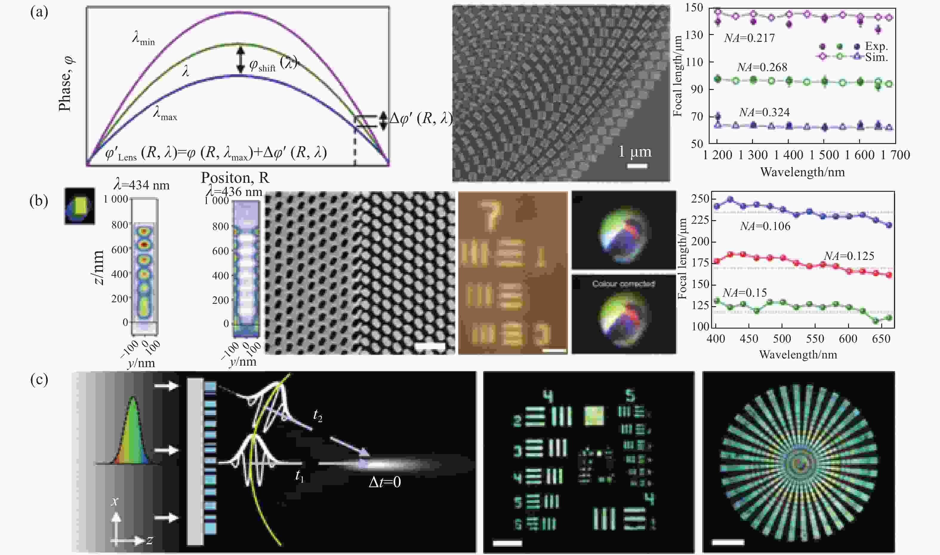
图 4 宽带消色差超透镜。(a)反射式宽带消色差超构透镜工作原理示意图,其扫描电子显微镜图像以及实验结果[80];(b)由氮化镓微纳柱和反结构制成的超构透镜在400 nm至660 nm范围内的成像效果[81];(c)将所需相位泰勒展开的原理图以及聚焦效果[82]
Figure 4. Broadband achromatic metalenses. (a) Schematic diagram of the working principle of the reflective broadband achromatic metalens, its scanning electron microscope image and experimental results[80]; (b) the imaging effect of the metalens made of gallium nitride nano pillars and reverse structure in the range of 400 nm to 660 nm[81]; (c) schematic diagram of the desired phase Taylor expansion and focusing effect[82]
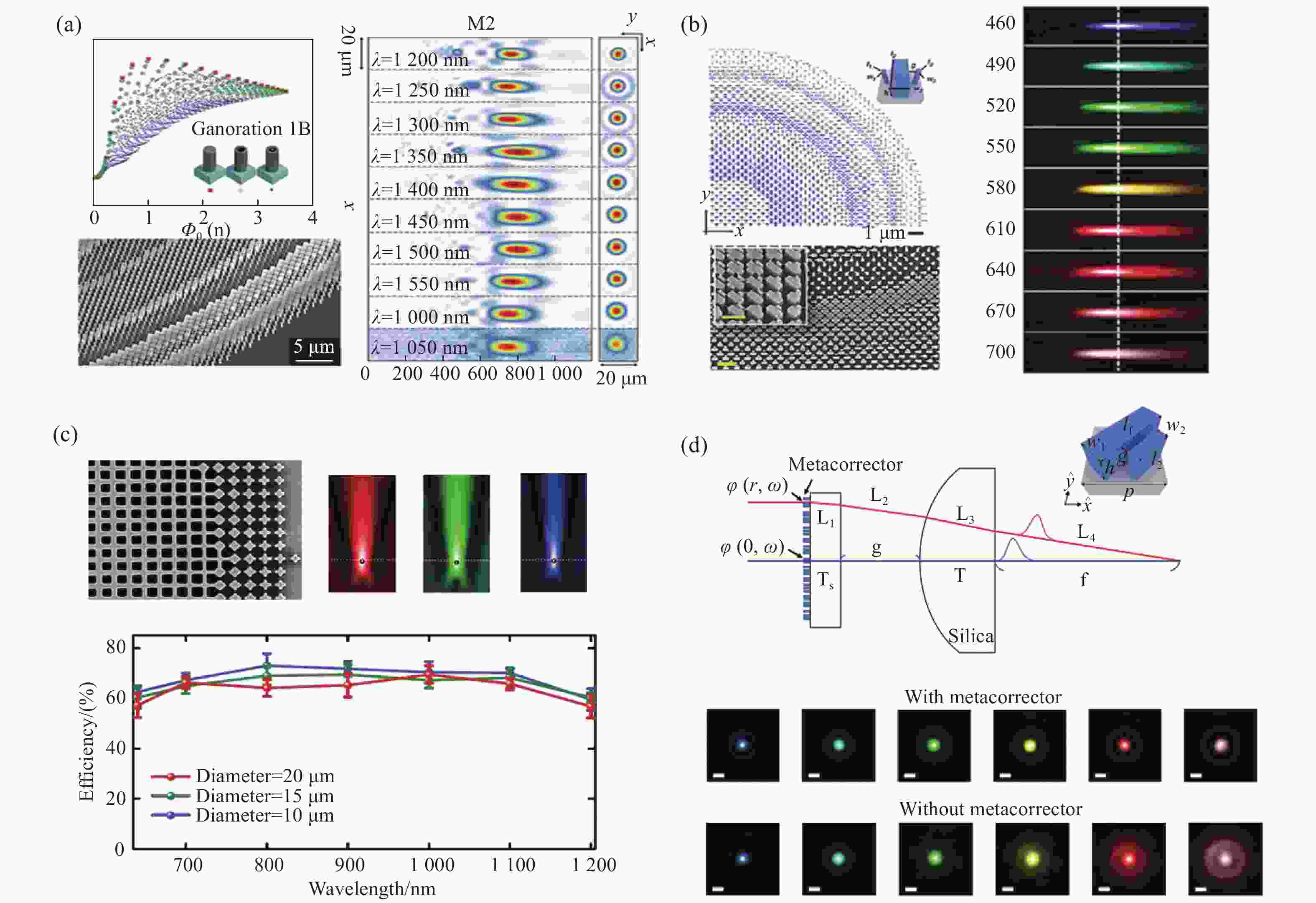
图 5 偏振不敏感的超构透镜。(a)在1200~1650 nm波长范围内偏振不敏感的宽带消色差超构透镜[83];(b) 在可见光波段的偏振不敏感超构透镜[84];(c) 渔网式结构的超构透镜实现宽带高效消色差[85];(d)通过结合超构表面和传统折射光学元件的宽带消色差器件[86]
Figure 5. Polarization-insensitive metalenses. (a) Polarization-insensitive broadband achromatic metalens in the wavelength range of 1200~1650 nm[83]; (b) polarization-insensitive metalens in the visible light band[84]; (c) the fishnet-like structure of the metalens realizes broadband high-efficiency achromatic aberration[85]; (d) broadband achromatic devices by combining metasurfaces and traditional refractive optical elements[86]
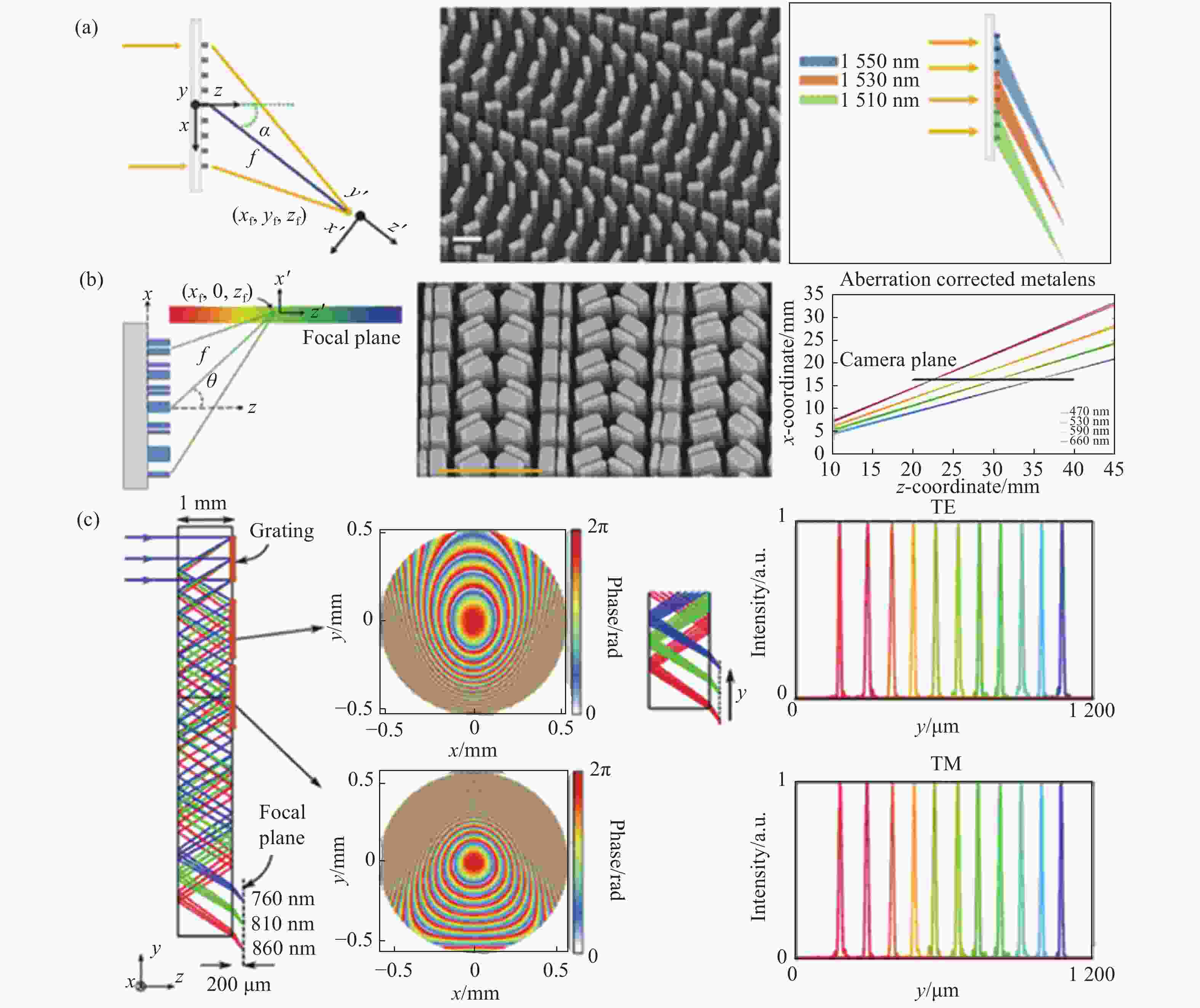

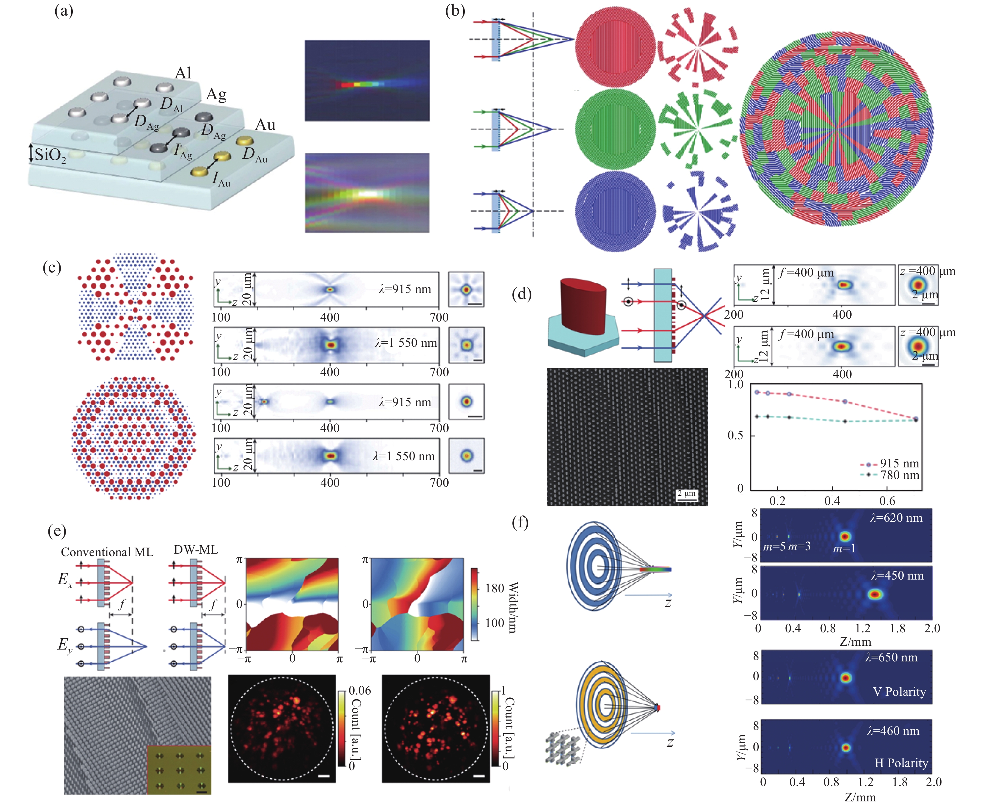
图 7 (a) 任意调控3个波长的复合式超构透镜[90];(b)构建超构单元色散数据库实现超构透镜任意色差调控[91];(c) 可见光波段多通道寻址[92]
Figure 7. (a) Compound metalens capable of adjusting three wavelengths arbitrarily[90]; (b) constructing a meta-atom dispersion database to realize arbitrary chromatic aberration control of metalens[91]; (c) color router in the visible light band[92]

图 8 (a) 任意调控3个波长的复合式超构透镜[93];(b) 宽带等离激元调制实现多色三维全息显示[94];(c) 毫米级高数值孔径超构透镜实现虚拟现实[95]
Figure 8. (a) Compound metalens with arbitrarily adjustable three wavelengths[93]; (b) broadband plasmon modulation realizes multi-color three-dimensional holographic display[94]; (c) millimeter-scale diameter and high numerical aperture metalens for virtual reality[95]

-
[1] JAHANI S, JACOB Z. All-dielectric metamaterials[J]. Nature Nanotechnology, 2016, 11(1): 23-36. doi: 10.1038/nnano.2015.304 [2] CHEBEN P, HALIR R, SCHMID J H, et al. Subwavelength integrated photonics[J]. Nature, 2018, 560(7720): 565-572. doi: 10.1038/s41586-018-0421-7 [3] KUZNETSOV A I, MIROSHNICHENKO A E, BRONGERSMA M L, et al. Optically resonant dielectric nanostructures[J]. Science, 2016, 354(6314): aag2472. doi: 10.1126/science.aag2472 [4] NICHOLLS L H, RODRÍGUEZ-FORTUÑO F J, NASIR M E, et al. Ultrafast synthesis and switching of light polarization in nonlinear anisotropic metamaterials[J]. Nature Photonics, 2017, 11(10): 628-633. doi: 10.1038/s41566-017-0002-6 [5] JAHANI S, KIM S, ATKINSON J, et al. Controlling evanescent waves using silicon photonic all-dielectric metamaterials for dense integration[J]. Nature Communications, 2018, 9(1): 1893. doi: 10.1038/s41467-018-04276-8 [6] STAUDE I, SCHILLING J. Metamaterial-inspired silicon nanophotonics[J]. Nature Photonics, 2017, 11(5): 274-284. doi: 10.1038/nphoton.2017.39 [7] SURJADI J U, GAO L B, DU H F, et al. Mechanical metamaterials and their engineering applications[J]. Advanced Engineering Materials, 2019, 21(3): 1800864. doi: 10.1002/adem.201800864 [8] HUANG L L, CHEN X ZH, MÜHLENBERND H, et al. Dispersionless phase discontinuities for controlling light propagation[J]. Nano Letters, 2012, 12(11): 5750-5755. doi: 10.1021/nl303031j [9] NI X J, WONG Z J, MREJEN M, et al. An ultrathin invisibility skin cloak for visible light[J]. Science, 2015, 349(6254): 1310-1314. doi: 10.1126/science.aac9411 [10] SHENG C, LIU H, WANG Y, et al. Trapping light by mimicking gravitational lensing[J]. Nature Photonics, 2013, 7(11): 902-906. doi: 10.1038/nphoton.2013.247 [11] HUANG Y W, LEE H W, SOKHOYAN R, et al. Gate-tunable conducting oxide metasurfaces[J]. Nano Letters, 2016, 16(9): 5319-5325. doi: 10.1021/acs.nanolett.6b00555 [12] KHORASANINEJAD M, CHEN W T, ZHU A Y, et al. Multispectral chiral imaging with a metalens[J]. Nano Letters, 2016, 16(7): 4595-4600. doi: 10.1021/acs.nanolett.6b01897 [13] WANG L, KRUK S, TANG H ZH, et al. Grayscale transparent metasurface holograms[J]. Optica, 2016, 3(12): 1504-1505. doi: 10.1364/OPTICA.3.001504 [14] DHARMAVARAPU R, IZUMI K I, KATAYAMA I, et al. Dielectric cross-shaped-resonator-based metasurface for vortex beam generation at mid-IR and THz wavelengths[J]. Nanophotonics, 2019, 8(7): 1263-1270. doi: 10.1515/nanoph-2019-0112 [15] MIA M B, AHMED S Z, AHMED I, et al. Exceptional coupling in photonic anisotropic metamaterials for extremely low waveguide crosstalk[J]. Optica, 2020, 7(8): 881-887. doi: 10.1364/OPTICA.394987 [16] SHERROTT M C, HON P W C, FOUNTAINE K T, et al. Experimental demonstration of > 230°phase modulation in gate-tunable graphene-gold reconfigurable mid-infrared metasurfaces[J]. Nano Letters, 2017, 17(5): 3027-3034. doi: 10.1021/acs.nanolett.7b00359 [17] RHO J, YE Z L, XIONG Y, et al. Spherical hyperlens for two-dimensional sub-diffractional imaging at visible frequencies[J]. Nature Communications, 2010, 1: 143. doi: 10.1038/ncomms1148 [18] SEGOVIA P, MARINO G, KRASAVIN A V, et al. Hyperbolic metamaterial antenna for second-harmonic generation tomography[J]. Optics Express, 2015, 23(24): 30730-30738. doi: 10.1364/OE.23.030730 [19] SHEKHAR P, PENDHARKER S, SAHASRABUDHE H, et al. Extreme ultraviolet plasmonics and Cherenkov radiation in silicon[J]. Optica, 2018, 5(12): 1590-1596. doi: 10.1364/OPTICA.5.001590 [20] SHALTOUT A M, SHALAEV V M, BRONGERSMA M L. Spatiotemporal light control with active metasurfaces[J]. Science, 2019, 364(6441): eaat3100. doi: 10.1126/science.aat3100 [21] ZHANG L, CHEN X Q, LIU SH, et al. Space-time-coding digital metasurfaces[J]. Nature Communications, 2018, 9(1): 4334. doi: 10.1038/s41467-018-06802-0 [22] CHEN SH Q, LI ZH CH, LIU W W, et al. From single-dimensional to multidimensional manipulation of optical waves with metasurfaces[J]. Advanced Materials, 2019, 31(16): 1802458. doi: 10.1002/adma.201802458 [23] LI Y, LI X, CHEN L W, et al. Orbital angular momentum multiplexing and demultiplexing by a single metasurface[J]. Advanced Optical Materials, 2017, 5(2): 1600502. doi: 10.1002/adom.201600502 [24] REMNEV M A, KLIMOV V V. Metasurfaces: a new look at Maxwell's equations and new ways to control light[J]. Physics-Uspekhi, 2018, 61(2): 157-190. doi: 10.3367/UFNe.2017.08.038192 [25] TSENG M L, HSIAO H H, CHU C H, et al. Metalenses: advances and applications[J]. Advanced Optical Materials, 2018, 6(18): 1800554. doi: 10.1002/adom.201800554 [26] GENEVET P, CAPASSO F, AIETA F, et al. Recent advances in planar optics: from plasmonic to dielectric metasurfaces[J]. Optica, 2017, 4(1): 139-152. doi: 10.1364/OPTICA.4.000139 [27] LI L, LIU Z X, REN X F, et al. Metalens-array-based high-dimensional and multiphoton quantum source[J]. Science, 2020, 368(6498): 1487-1490. doi: 10.1126/science.aba9779 [28] YU N F, GENEVET P, KATS M A, et al. Light propagation with phase discontinuities: generalized laws of reflection and refraction[J]. Science, 2011, 334(6054): 333-337. doi: 10.1126/science.1210713 [29] HUANG T Y, GROTE R R, MANN S A, et al. A monolithic immersion metalens for imaging solid-state quantum emitters[J]. Nature Communications, 2019, 10(1): 2392. doi: 10.1038/s41467-019-10238-5 [30] YUE F Y, WEN D D, XIN J T, et al. Vector vortex beam generation with a single plasmonic metasurface[J]. ACS Photonics, 2016, 3(9): 1558-1563. doi: 10.1021/acsphotonics.6b00392 [31] ZHU W M, SONG Q H, YAN L B, et al. A flat lens with tunable phase gradient by using random access reconfigurable metamaterial[J]. Advanced Materials, 2015, 27(32): 4739-4743. doi: 10.1002/adma.201501943 [32] KHORASANINEJAD M, CHEN W T, DEVLIN R C, et al. Metalenses at visible wavelengths: diffraction-limited focusing and subwavelength resolution imaging[J]. Science, 2016, 352(6290): 1190-1194. doi: 10.1126/science.aaf6644 [33] PU M B, LI X, MA X L, et al. Catenary optics for achromatic generation of perfect optical angular momentum[J]. Science Advances, 2015, 1(9): e1500396. doi: 10.1126/sciadv.1500396 [34] HSIAO H H, CHEN Y H, LIN R J, et al. Integrated-resonant units: integrated resonant unit of metasurfaces for broadband efficiency and phase manipulation (advanced optical materials 12/2018)[J]. Advanced Optical Materials, 2018, 6(12): 1870047. doi: 10.1002/adom.201870047 [35] GOLDYS E M, GODLEWSKI M, LANGER R, et al. Analysis of the red optical emission in cubic GaN grown by molecular-beam epitaxy[J]. Physical Review B, 1999, 60(8): 5464-5469. doi: 10.1103/PhysRevB.60.5464 [36] HSIAO H H, CHU C H, TSAI D P. Fundamentals and applications of metasurfaces[J]. Small Methods, 2017, 1(4): 1600064. doi: 10.1002/smtd.201600064 [37] YU N F, CAPASSO F. Flat optics with designer metasurfaces[J]. Nature Materials, 2014, 13(2): 139-150. doi: 10.1038/nmat3839 [38] WU P C, TSAI W Y, CHEN W T, et al. Versatile polarization generation with an aluminum plasmonic metasurface[J]. Nano Letters, 2017, 17(1): 445-452. doi: 10.1021/acs.nanolett.6b04446 [39] LI L, LI T, TANG X M, et al. Plasmonic polarization generator in well-routed beaming[J]. Light:Science &Applications, 2015, 4(9): e330. [40] WU P C, ZHU W M, SHEN ZH X, et al. Broadband wide-angle multifunctional polarization converter via liquid-metal-based metasurface[J]. Advanced Optical Materials, 2017, 5(7): 1600938. doi: 10.1002/adom.201600938 [41] HUANG L L, MÜHLENBERND H, LI X W, et al. Broadband hybrid holographic multiplexing with geometric metasurfaces[J]. Advanced Materials, 2015, 27(41): 6444-6449. doi: 10.1002/adma.201502541 [42] WU P C, PAPASIMAKIS N, TSAI D P. Self-affine graphene metasurfaces for tunable broadband absorption[J]. Physical Review Applied, 2016, 6(4): 044019. doi: 10.1103/PhysRevApplied.6.044019 [43] THYAGARAJAN K, SOKHOYAN R, ZORNBERG L, et al. Millivolt modulation of plasmonic metasurface optical response via ionic conductance[J]. Advanced Materials, 2017, 29(31): 1701044. doi: 10.1002/adma.201701044 [44] KHORASANINEJAD M, AIETA F, KANHAIYA P, et al. Achromatic metasurface lens at telecommunication wavelengths[J]. Nano Letters, 2015, 15(8): 5358-5362. doi: 10.1021/acs.nanolett.5b01727 [45] STRIKWERDA A C, SLEASMAN T, ANDERSON W, et al. Sub-wavelength focusing in inhomogeneous media with a metasurface near field plate[J]. Sensors (Basel) , 2019, 19(20): 4534. doi: 10.3390/s19204534 [46] KHORASANINEJAD M, CAPASSO F. Metalenses: versatile multifunctional photonic components[J]. Science, 2017, 358(6367): eaam8100. doi: 10.1126/science.aam8100 [47] EPSTEIN A, ELEFTHERIADES G V. Huygens’ metasurfaces via the equivalence principle: design and applications[J]. Journal of the Optical Society of America B, 2016, 33(2): A31-A50. doi: 10.1364/JOSAB.33.000A31 [48] CHEN H Y, WANG J F, MA H, et al. Ultra-wideband polarization conversion metasurfaces based on multiple plasmon resonances[J]. Journal of Applied Physics, 2014, 115(15): 154504. doi: 10.1063/1.4869917 [49] DING X M, MONTICONE F, ZHANG K, et al. Ultrathin pancharatnam-berry metasurface with maximal cross-polarization efficiency[J]. Advanced Materials, 2015, 27(7): 1195-1200. doi: 10.1002/adma.201405047 [50] CHEN W T, YANG K Y, WANG C M, et al. High-efficiency broadband meta-hologram with polarization-controlled dual images[J]. Nano Letters, 2014, 14(1): 225-230. doi: 10.1021/nl403811d [51] DING F, CHANG B D, WEI Q SH, et al. Versatile polarization generation and manipulation using dielectric metasurfaces[J]. Laser &Photonics Reviews, 2020, 14(11): 2000116. [52] RUBIN N A, D'AVERSA G, CHEVALIER P, et al. Matrix Fourier optics enables a compact full-Stokes polarization camera[J]. Science, 2019, 365(6448): eaax1839. doi: 10.1126/science.aax1839 [53] ARBABI E, KAMALI S M, ARBABI A, et al. Full-stokes imaging polarimetry using dielectric metasurfaces[J]. ACS Photonics, 2018, 5(8): 3132-3140. doi: 10.1021/acsphotonics.8b00362 [54] MUELLER J P B, RUBIN N A, DEVLIN R C, et al. Metasurface polarization optics: independent phase control of arbitrary orthogonal states of polarization[J]. Physical Review Letters, 2017, 118(11): 113901. doi: 10.1103/PhysRevLett.118.113901 [55] HUANG Y W, CHEN W T, TSAI W Y, et al. Aluminum plasmonic multicolor meta-hologram[J]. Nano Letters, 2015, 15(5): 3122-3127. doi: 10.1021/acs.nanolett.5b00184 [56] WEN D D, YUE F Y, LI G X, et al. Helicity multiplexed broadband metasurface holograms[J]. Nature Communications, 2015, 6: 8241. doi: 10.1038/ncomms9241 [57] LI X, CHEN L W, LI Y, et al. Multicolor 3D meta-holography by broadband plasmonic modulation[J]. Science Advances, 2016, 2(11): e1601102. doi: 10.1126/sciadv.1601102 [58] WAN W Q, QIAO W, HUANG W B, et al. Multiview holographic 3D dynamic display by combining a nano-grating patterned phase plate and LCD[J]. Optics Express, 2017, 25(2): 1114-1122. doi: 10.1364/OE.25.001114 [59] FATTAL D, PENG ZH, TRAN T, et al. A multi-directional backlight for a wide-angle, glasses-free three-dimensional display[J]. Nature, 2013, 495(7441): 348-351. doi: 10.1038/nature11972 [60] LIPPMANN G. Épreuves réversibles donnant la sensation du relief[J]. Journal de Physique Théorique et Appliquée, 1908, 7(1): 821-825. [61] ADELSON E H, WANG J Y A. Single lens stereo with a plenoptic camera[J]. IEEE Transactions on Pattern Analysis and Machine Intelligence, 1992, 14(2): 99-106. doi: 10.1109/34.121783 [62] BOK Y, JEON H G, KWEON I S. Geometric calibration of micro-lens-based light field cameras using line features[J]. IEEE Transactions on Pattern Analysis and Machine Intelligence, 2017, 39(2): 287-300. doi: 10.1109/TPAMI.2016.2541145 [63] SHEN K C, KU CH T, HSIEH C, et al. Deep-ultraviolet hyperbolic metacavity laser[J]. Advanced Materials, 2018, 30(21): 1706918. doi: 10.1002/adma.201706918 [64] GONGORA J S T, MIROSHNICHENKO A E, KIVSHAR Y S, et al. Anapole nanolasers for mode-locking and ultrafast pulse generation[J]. Nature Communications, 2017, 8: 15535. doi: 10.1038/ncomms15535 [65] ZHANG Q, LI G Y, LIU X F, et al. A room temperature low-threshold ultraviolet plasmonic nanolaser[J]. Nature Communications, 2014, 5: 4953. doi: 10.1038/ncomms5953 [66] ZHANG W X, XIE X, HAO H M, et al. Low-threshold topological nanolasers based on the second-order corner state[J]. Light:Science &Applications, 2020, 9: 109. [67] MELENTIEV P, KALMYKOV A, GRITCHENKO A, et al. Plasmonic nanolaser for intracavity spectroscopy and sensorics[J]. Applied Physics Letters, 2017, 111(21): 213104. doi: 10.1063/1.5003655 [68] SWEATT W C. Achromatic triplet using holographic optical elements[J]. Applied Optics, 1977, 16(5): 1390-1391. doi: 10.1364/AO.16.001390 [69] AVAYU O, ALMEIDA E, PRIOR Y, et al. Composite functional metasurfaces for multispectral achromatic optics[J]. Nature Communications, 2017, 8: 14992. doi: 10.1038/ncomms14992 [70] LIN D M, HOLSTEEN A L, MAGUID E, et al. Photonic multitasking interleaved Si nanoantenna phased array[J]. Nano Letters, 2016, 16(12): 7671-7676. doi: 10.1021/acs.nanolett.6b03505 [71] ARBABI E, ARBABI A, KAMALI S M, et al. Multiwavelength metasurfaces through spatial multiplexing[J]. Scientific Reports, 2016, 6: 32803. doi: 10.1038/srep32803 [72] ARBABI E, ARBABI A, KAMALI S M, et al. High efficiency double-wavelength dielectric metasurface lenses with dichroic birefringent meta-atoms[J]. Optics Express, 2016, 24(16): 18468-18477. doi: 10.1364/OE.24.018468 [73] ARBABI E, LI J Q, HUTCHINS R J, et al. Two-photon microscopy with a double-wavelength metasurface objective lens[J]. Nano Letters, 2018, 18(8): 4943-4948. doi: 10.1021/acs.nanolett.8b01737 [74] EISENBACH O, AVAYU O, DITCOVSKI R, et al. Metasurfaces based dual wavelength diffractive lenses[J]. Optics Express, 2015, 23(4): 3928-3936. doi: 10.1364/OE.23.003928 [75] WANG P, MOHAMMAD N, MENON R. Chromatic-aberration-corrected diffractive lenses for ultra-broadband focusing[J]. Scientific Reports, 2016, 6: 21545. doi: 10.1038/srep21545 [76] HU J T, LIU CH H, REN X CH, et al. Plasmonic lattice lenses for multiwavelength achromatic focusing[J]. ACS Nano, 2016, 10(11): 10275-10282. doi: 10.1021/acsnano.6b05855 [77] ZHAO Z Y, PU M B, GAO H, et al. Multispectral optical metasurfaces enabled by achromatic phase transition[J]. Scientific Reports, 2015, 5: 15781. doi: 10.1038/srep15781 [78] KHORASANINEJAD M, SHI Z, ZHU A Y, et al. Achromatic metalens over 60 nm bandwidth in the visible and metalens with reverse chromatic dispersion[J]. Nano Letters, 2017, 17(3): 1819-1824. doi: 10.1021/acs.nanolett.6b05137 [79] ARBABI E, ARBABI A, KAMALI S M, et al. Controlling the sign of chromatic dispersion in diffractive optics with dielectric metasurfaces[J]. Optica, 2017, 4(6): 625-632. doi: 10.1364/OPTICA.4.000625 [80] WANG SH M, WU P C, SU V C, et al. Broadband achromatic optical metasurface devices[J]. Nature Communications, 2017, 8(1): 187. doi: 10.1038/s41467-017-00166-7 [81] WANG SH M, WU P C, SU V C, et al. A broadband achromatic metalens in the visible[J]. Nature Nanotechnology, 2018, 13(3): 227-232. doi: 10.1038/s41565-017-0052-4 [82] CHEN W T, ZHU A Y, SANJEEV V, et al. A broadband achromatic metalens for focusing and imaging in the visible[J]. Nature Nanotechnology, 2018, 13(3): 220-226. doi: 10.1038/s41565-017-0034-6 [83] SHRESTHA S, OVERVIG A C, LU M, et al. Broadband achromatic dielectric metalenses[J]. Light:Science &Applications, 2018, 7: 85. [84] CHEN W T, ZHU A Y, SISLER J, et al. A broadband achromatic polarization-insensitive metalens consisting of anisotropic nanostructures[J]. Nature Communications, 2019, 10(1): 355. doi: 10.1038/s41467-019-08305-y [85] NDAO A, HSU L, HA J, et al. Octave bandwidth photonic fishnet-achromatic-metalens[J]. Nature Communications, 2020, 11(1): 3205. doi: 10.1038/s41467-020-17015-9 [86] CHEN W T, ZHU A Y, SISLER J, et al. Broadband achromatic metasurface-refractive optics[J]. Nano Letters, 2018, 18(12): 7801-7808. doi: 10.1021/acs.nanolett.8b03567 [87] KHORASANINEJAD M, CHEN W T, OH J, et al. Super-dispersive off-axis meta-lenses for compact high resolution spectroscopy[J]. Nano Letters, 2016, 16(6): 3732-3737. doi: 10.1021/acs.nanolett.6b01097 [88] ZHU A Y, CHEN W T, SISLER J, et al. Compact aberration‐corrected spectrometers in the visible using dispersion‐tailored metasurfaces[J]. Advanced Optical Materials, 2019, 7(14): 1801144. doi: 10.1002/adom.201801144 [89] FARAJI-DANA M, ARBABI E, ARBABI A, et al. Compact folded metasurface spectrometer[J]. Nature Communications, 2018, 9(1): 4196. doi: 10.1038/s41467-018-06495-5 [90] LI K, GUO Y H, PU M B, et al. Dispersion controlling meta-lens at visible frequency[J]. Optics Express, 2017, 25(18): 21419-21427. doi: 10.1364/OE.25.021419 [91] SISLER J, CHEN W T, ZHU A Y, et al. Controlling dispersion in multifunctional metasurfaces[J]. APL Photonics, 2020, 5(5): 056107. doi: 10.1063/1.5142637 [92] CHEN B H, WU P C, SU V C, et al. GaN metalens for pixel-level full-color routing at visible light[J]. Nano Letters, 2017, 17(10): 6345-6352. doi: 10.1021/acs.nanolett.7b03135 [93] WANG B, DONG F L, LI Q T, et al. Visible-frequency dielectric metasurfaces for multiwavelength achromatic and highly dispersive holograms[J]. Nano Letters, 2016, 16(8): 5235-5240. doi: 10.1021/acs.nanolett.6b02326 [94] ROTH D J, JIN M K, MINOVICH A E, et al. 3D full-color image projection based on reflective metasurfaces under incoherent illumination[J]. Nano Letters, 2020, 20(6): 4481-4486. doi: 10.1021/acs.nanolett.0c01273 [95] LI ZH Y, LIN P, HUANG Y W, et al. Meta-optics achieves RGB-achromatic focusing for virtual reality[J]. Science Advances, 2021, 7(5): eabe4458. doi: 10.1126/sciadv.abe4458 [96] CHEN CH, SONG W G, CHEN J W, et al. Spectral tomographic imaging with aplanatic metalens[J]. Light:Science &Applications, 2019, 8: 99. [97] PAHLEVANINEZHAD H, KHORASANINEJAD M, HUANG Y W, et al. Nano-optic endoscope for high-resolution optical coherence tomography in vivo[J]. Nature Photonics, 2018, 12(9): 540-547. doi: 10.1038/s41566-018-0224-2 [98] LIN R J, SU V C, WANG SH M, et al. Achromatic metalens array for full-colour light-field imaging[J]. Nature Nanotechnology, 2019, 14(3): 227-231. doi: 10.1038/s41565-018-0347-0 [99] FAN ZH B, QIU H Y, ZHANG H L, et al. A broadband achromatic metalens array for integral imaging in the visible[J]. Light:Science &Applications, 2019, 8: 67. -


 下载:
下载:


计量
- 文章访问数: 3277
- HTML全文浏览量: 1307
- PDF下载量: 686
- 被引次数: 0
