


Damage characteristics of a 532 nm picosecond pulse laser on monocrystalline silicon
-
摘要: 随着光电对抗和超短脉冲金宝搏188软件怎么用 技术的发展,研究超短脉冲金宝搏188软件怎么用 与单晶硅相互作用具有非常重要的理论和实际意义。为了进一步明确532 nm皮秒脉冲金宝搏188软件怎么用 对单晶硅的损伤机理,本文开展了532 nm皮秒脉冲金宝搏188软件怎么用 辐照单晶硅的损伤效应实验研究,测定了损伤阈值,明确了损伤机理,探讨了低通量下的脉冲累积效应。首先,利用波长为532 nm、脉冲宽度为30 ps的金宝搏188软件怎么用 器和金相显微镜,基于1-on-1的金宝搏188软件怎么用 损伤测试方法,测定了单晶硅的零损伤概率阈值为0.52 J/cm2;其次,研究了皮秒金宝搏188软件怎么用 辐照单晶硅在不同金宝搏188软件怎么用 能量密度下的损伤形貌,发现532 nm皮秒脉冲金宝搏188软件怎么用 对单晶硅的损伤表现为热影响损伤和等离子体冲击损伤,随着金宝搏188软件怎么用 能量密度的增大,按主要的损伤机制可将损伤程度分为:热影响(0.52~3 J/cm2)、热烧蚀(3~50 J/cm2)和等离子烧蚀(>50 J/cm2),且不同情况下,损伤面积随金宝搏188软件怎么用 能量密度分别对应不同的增长规律;最后,研究了低通量下多脉冲的累积效应,发现在0.52 J/cm2的金宝搏188软件怎么用 能量密度下,连续辐照16个脉冲时表面形成热影响区,验证了多脉冲的累积效应可以降低单晶硅的金宝搏188软件怎么用 损伤阈值。
-
关键词:
- 皮秒脉冲金宝搏188软件怎么用 /
- 单晶硅 /
- 损伤阈值 /
- 累积效应 /
- 损伤特性
Abstract: With the development of optoelectronic countermeasures and ultrashort pulse laser technology, the study of the interaction between ultrashort pulse laser and monocrystalline silicon has a very important theoretical and practical significance. In order to further clarify the damage mechanism of 532 nm picosecond pulsed laser on monocrystalline silicon, we have conducted an experimental study to measure the damage threshold, clarify the damage mechanism, and discuss the pulse accumulation effect at low flux. Firstly, using a laser with a wavelength of 532 nm, a pulse width of 30 ps and a metallurgical microscope based on the 1-on-1 laser damage test method, the zero damage probability threshold is determined to be 0.52 J/cm2. Secondly, the damage effect of a picosecond laser irradiated on monocrystalline silicon was studied under different laser fluxes, and it was found that the damage of 532 nm picosecond laser to monocrystalline silicon is manifested as heated-effect damage and plasma impact damage. The increase in energy density can be divided into three stages according to the main damage mechanism: thermal effect (0.52~3 J/cm2), thermal ablation (3~50 J/cm2) and plasma effect (>50 J/cm2), and the damaged areas are corresponded to different growth laws with the laser energy density, respectively. Finally, an experiment for the multi-pulse cumulative effect was carried out at a low laser flux and it was found that at a laser energy density of 0.52 J/cm2, the surface was irradiated continuously for 16 shots. The formation of a heat-affected zone confirms that the cumulative effect of multiple pulses can lower the laser damage threshold on monocrystalline silicon. -
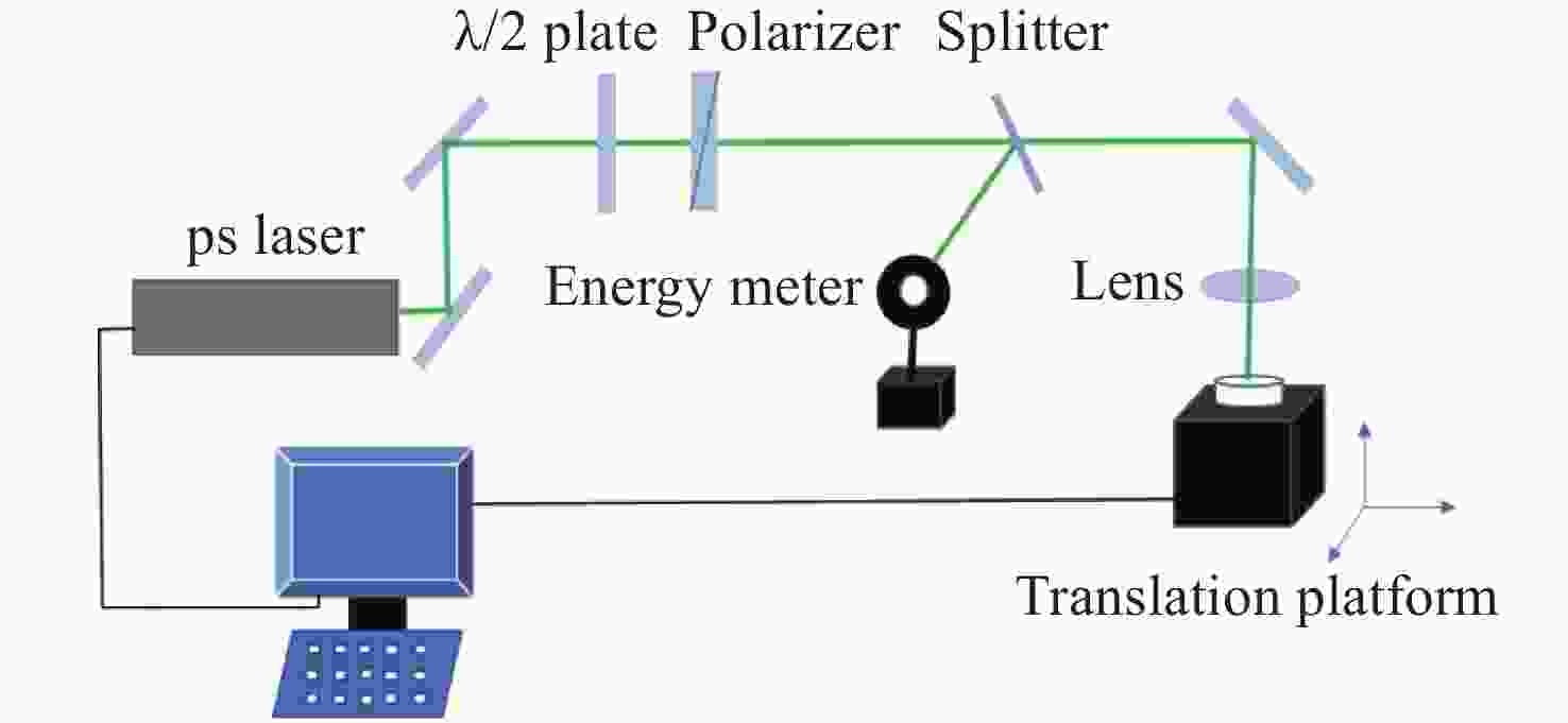
图 1 皮秒金宝搏188软件怎么用 诱导损伤实验装置图
Figure 1. Schematic diagram of the picosecond laser induced damage experiment setup
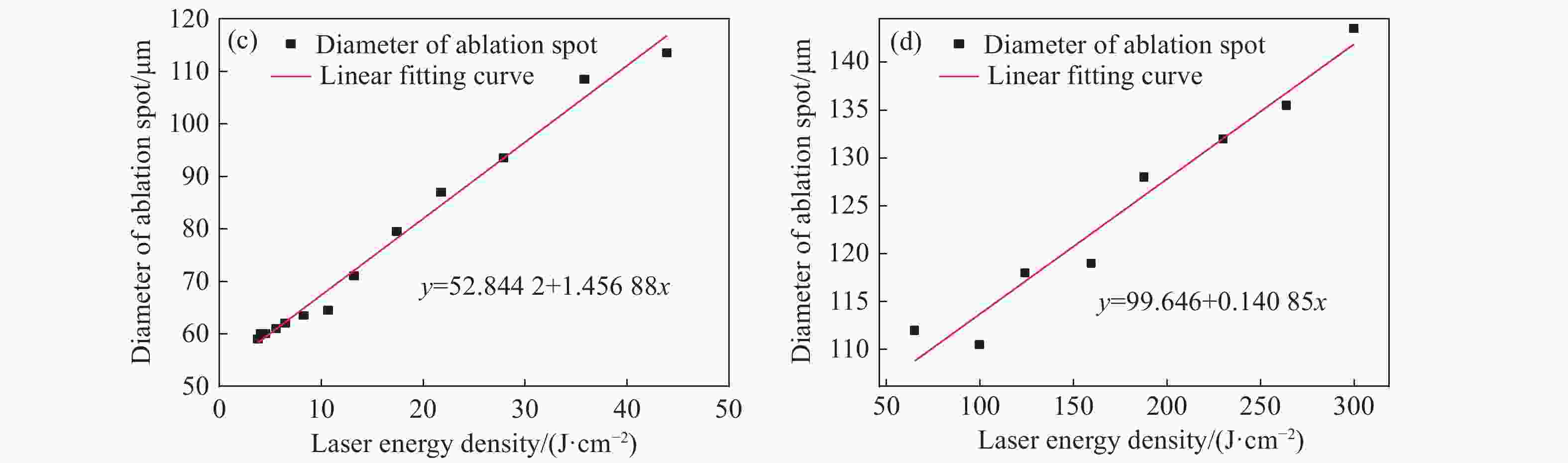
图 2 损伤区域尺寸随金宝搏188软件怎么用 能量密度的变化规律
Figure 2. The size of the damaged area changes with the laser’s energy density
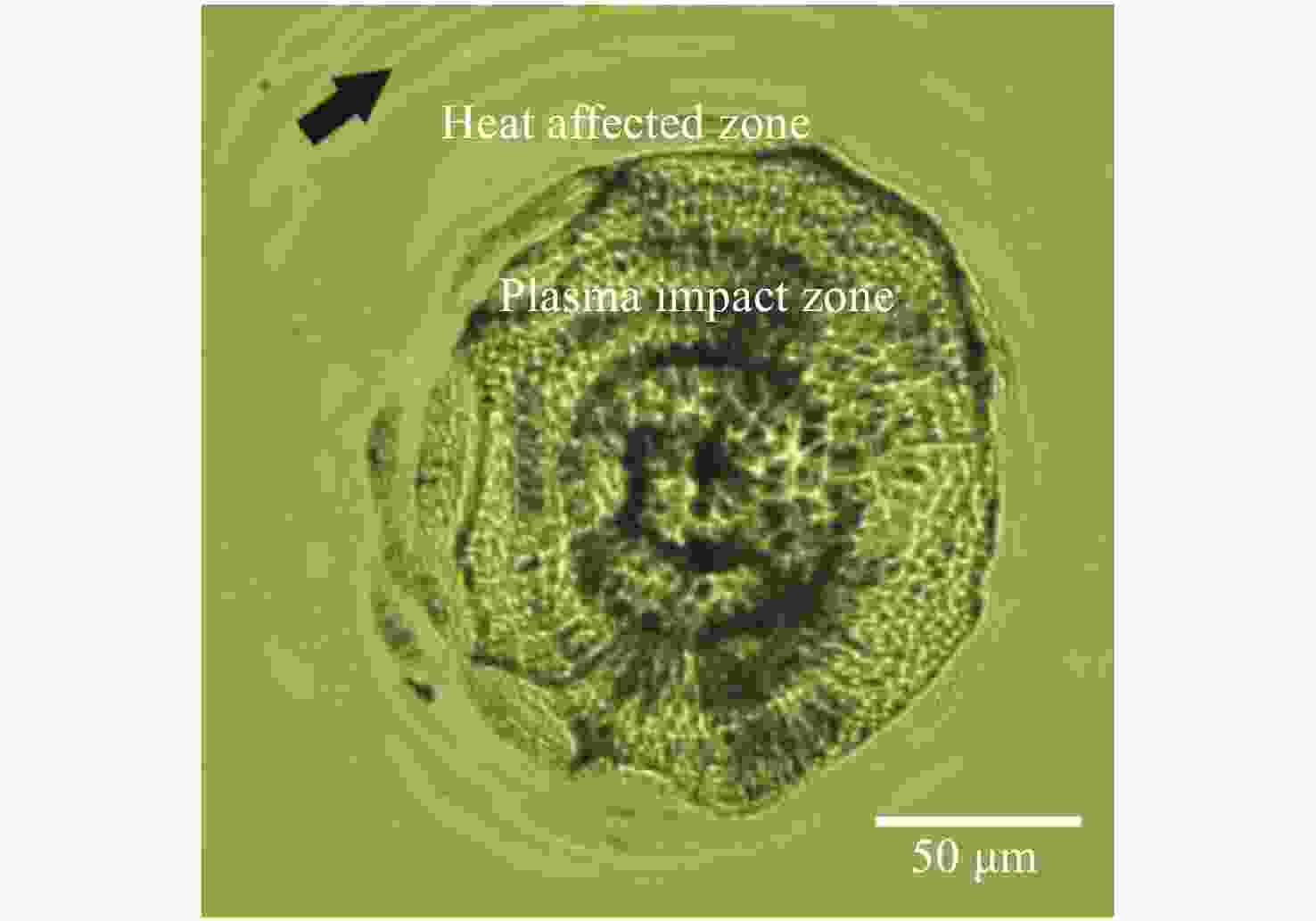
图 4 302 J/cm2能量密度的损伤形貌图
Figure 4. Damage morphography at the energy density of 302 J/cm2
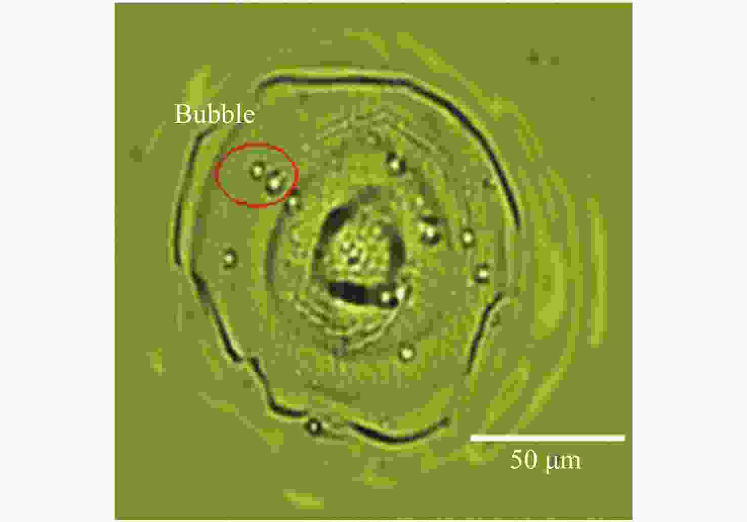
图 5 能量密度为21.9 J/cm2的损伤形貌图
Figure 5. Damage morpography at the energy density of 21.9 J/cm2

图 6 能量密度为3.04 J/cm2的损伤形貌图
Figure 6. Damage morphography at the energy density of 3.04 J/cm2

图 7 能量密度为0.52、1.07 J/cm2时脉冲累积效应的损伤形貌
Figure 7. Damage morphography from the pulse accumulation effect at the energy densities of 0.52 J/cm2、1.07 J/cm2
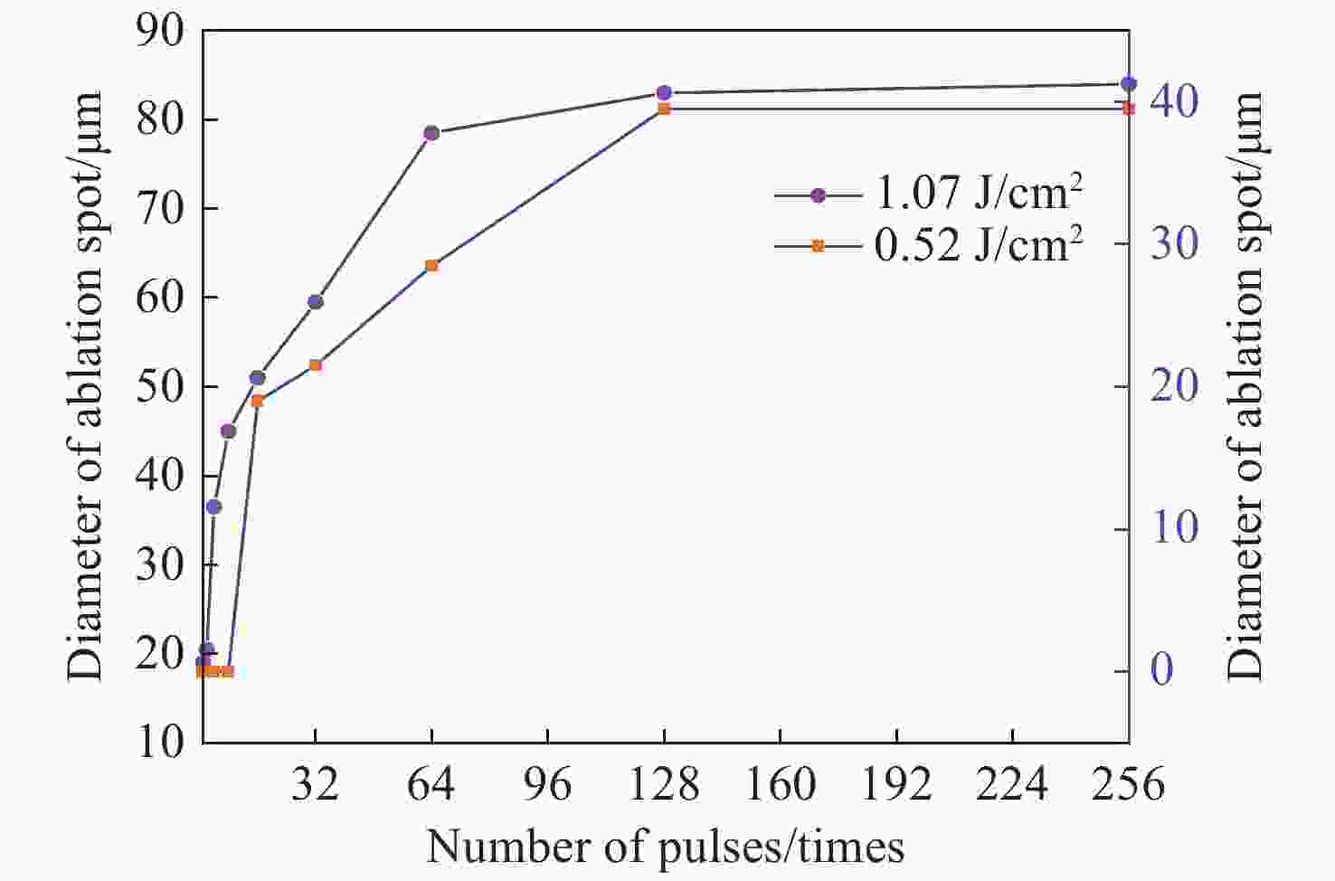
图 8 烧蚀区域尺寸随脉冲数量的变化规律
Figure 8. Variation of the ablation zone size with the number of pulses
-
[1] XIE CH, MEYER R, FROEHLY L, et al. In-situ diagnostic of femtosecond laser probe pulses for high resolution ultrafast imaging[J]. Light:Science &Applications, 2021, 10(1): 126. [2] JIANG L, WANG A D, LI B, et al. Electrons dynamics control by shaping femtosecond laser pulses in micro/nanofabrication: modeling, method, measurement and application[J]. Light:Science &Applications, 2018, 7(2): 17134. [3] MALINAUSKAS M, ŽUKAUSKAS A, HASEGAWA S, et al. Ultrafast laser processing of materials: from science to industry[J]. Light:Science &Applications, 2016, 5(8): e16133. [4] LIU Y, LIU L SH, TANG W, et al. Experimental study on the damage of optical materials by out of band composite laser[J]. Applied Sciences, 2020, 10(10): 3578. doi: 10.3390/app10103578 [5] FINGER J, BORNSCHLEGEL B, REININGHAUS M, et al. Heat input and accumulation for ultrashort pulse processing with high average power[J]. Advanced Optical Technologies, 2018, 7(3): 145-155. doi: 10.1515/aot-2018-0008 [6] CHICHKOV B N, MOMMA C, NOLTE S, et al. Femtosecond, picosecond and nanosecond laser ablation of solids[J]. Applied Physics A, 1996, 63(2): 109-115. doi: 10.1007/BF01567637 [7] MERKLE L D, BASS M, SWIMM R T. Erratum: multiple pulse laser-induced bulk damage in crystalline and fused quartz at 1.064 and 0.532 õm[J]. Optical Engineering, 1986, 25(1): 251196. doi: 10.1117/12.7973801 [8] MEYER J R, KRUER M R, BARTOLI F J. Optical heating in semiconductors: laser damage in Ge, Si, InSb, and GaAs[J]. Journal of Applied Physics, 1980, 51(10): 5513-5522. doi: 10.1063/1.327469 [9] RUBLACK T, HARTNAUER S, MERGNER M, et al. Mechanism of selective removal of transparent layers on semiconductors using ultrashort laser pulses[J]. Proceedings of SPIE, 2012, 8247: 82470Z. doi: 10.1117/12.905741 [10] SMIRNOV N A, KUDRYASHOV S I, RUDENKO A A, et al. Pulsewidth and ambient medium effects during ultrashort-pulse laser ablation of silicon in air and water[J]. Applied Surface Science, 2021, 562: 150243. doi: 10.1016/j.apsusc.2021.150243 [11] 张明鑫, 李志明, 聂劲松, 等. 多脉冲飞秒金宝搏188软件怎么用 烧蚀硅的热累积效应[J]. 光电子技术,2018,38(4):224-230.ZHANG M X, LI ZH M, NIE J S, et al. Heat accumulation effect of multipulse femtosecond laser ablation of silicon[J]. Optoelectronic Technology, 2018, 38(4): 224-230. (in Chinese) [12] WANG X, SHEN ZH H, LU J, et al. Laser-induced damage threshold of silicon in millisecond, nanosecond, and picosecond regimes[J]. Journal of Applied Physics, 2010, 108(3): 033103. doi: 10.1063/1.3466996 [13] VAN WOERKOM T A, PERRAM G P, DOLASINSKI B D, et al. Picosecond laser ablation of metals and semiconductors with low-transverse order Gaussian beams[J]. Optical Engineering, 2020, 60(3): 031002. [14] SHAHEEN M E, GAGNON J E, FRYER B J. Studies on laser ablation of silicon using near IR picosecond and deep UV nanosecond lasers[J]. Optics and Lasers in Engineering, 2019, 119: 18-25. doi: 10.1016/j.optlaseng.2019.02.003 [15] THORSTENSEN J, FOSS S E. Investigation of depth of laser damage to silicon as function of wavelength and pulse duration[J]. Energy Procedia, 2013, 38: 794-800. doi: 10.1016/j.egypro.2013.07.348 [16] 郑长彬, 邵俊峰, 李雪雷, 等. 飞秒脉冲金宝搏188软件怎么用 对硅基多层膜损伤特性[J]. 中国光学,2019,12(2):371-381. doi: 10.3788/co.20191202.0371ZHENG CH B, SHAO J F, LI X L, et al. Femtosecond pulsed laser induced damage characteristics on Si-based multi-layer film[J]. Chinese Optics, 2019, 12(2): 371-381. (in Chinese) doi: 10.3788/co.20191202.0371 [17] 邵俊峰, 郭劲, 王挺峰. 飞秒金宝搏188软件怎么用 与硅的相互作用过程理论研究[J]. 红外与金宝搏188软件怎么用 工程,2014,43(8):2419-2424. doi: 10.3969/j.issn.1007-2276.2014.08.005SHAO J F, GUO J, WANG T F. Theoretical research on dynamics of femto-second laser ablation crystal silicon[J]. Infrared and Laser Engineering, 2014, 43(8): 2419-2424. (in Chinese) doi: 10.3969/j.issn.1007-2276.2014.08.005 [18] MCDONALD J P, MISTRY V R, RAY K E, et al. Femtosecond pulsed laser direct write production of nano- and microfluidic channels[J]. Applied Physics Letters, 2006, 88(18): 183113. doi: 10.1063/1.2201620 [19] BENOCCI R, BATANI D, ROMAN H E. Incubation models for under-threshold laser ablation with thermal dissipation[J]. Applied Physics B, 2019, 125(2): 22. doi: 10.1007/s00340-019-7132-0 [20] KÜPER S, STUKE M. UV-excimer-laser ablation of polymethylmethacrylate at 248 nm: characterization of incubation sites with Fourier transform IR- and UV-spectroscopy[J]. Applied Physics A, 1989, 49(2): 211-215. doi: 10.1007/BF00616301 [21] KÜPER S, STUKE M. Femtosecond UV excimer laser ablation[J]. Applied Physics B, 1987, 44(4): 199-204. doi: 10.1007/BF00692122 [22] VAN DER LINDEN S, HAGMEIJER R, RÖMER G R B E. Picosecond pulsed underwater laser ablation of silicon and stainless steel: comparing crater analysis methods and analysing dependence of crater characteristics on water layer thickness[J]. Applied Surface Science, 2021, 540: 148005. doi: 10.1016/j.apsusc.2020.148005 -


 下载:
下载:


计量
- 文章访问数: 1421
- HTML全文浏览量: 603
- PDF下载量: 223
- 被引次数: 0
