Multiple Fano resonance properties of nanoring-heptamer metal-dielectric structures
doi: 10.37188/CO.2022-0170
-
摘要:
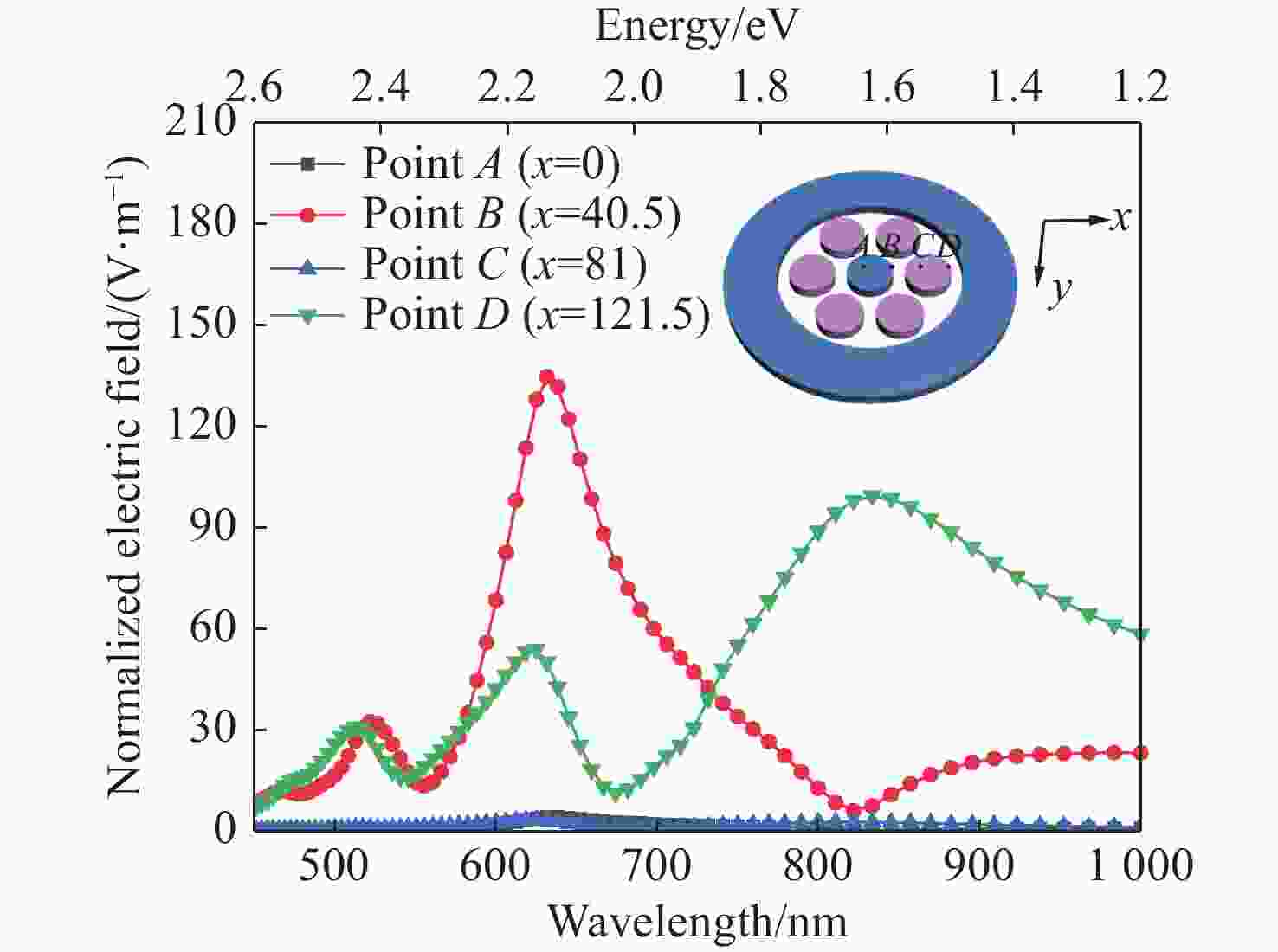
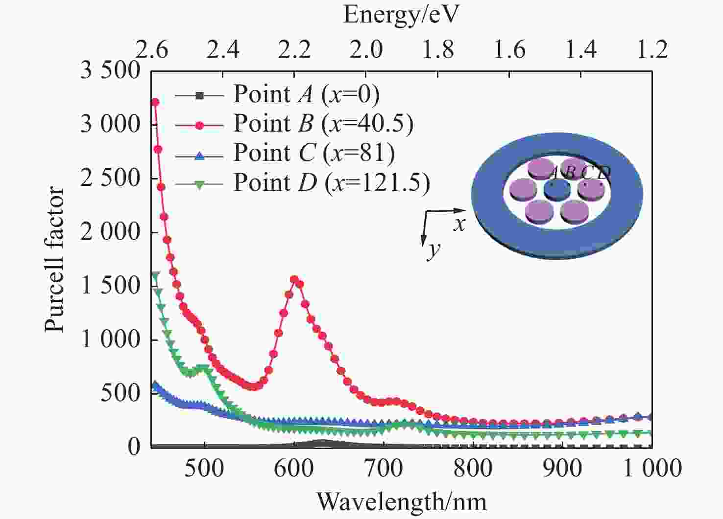
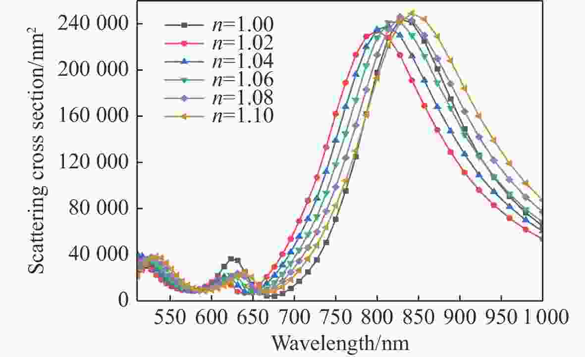
为实现可调谐的多重Fano共振特性及设计高灵敏度折射率传感器,本文提出一种纳米环-七聚体金属-介电纳米天线结构,利用有限元方法(Finite Element Method, FEM)研究了Fano共振特性的影响因素和变化规律。研究表明,纳米环-七聚体金属-介电纳米天线的Fano共振特性对高度、入射角度和结构间隙的变化非常敏感;纳米天线的电场强度和电偶极源激发下的珀赛尔系数(Purcell factor, PF)可达134.74 V/m和3214,使得纳米天线中心位置附近的电场强度得到大幅增强;复合纳米天线结构具有较高的灵敏度S和品质因数FOM,分别为1400 nm/RIU和17 RIU−1,可作为评价高灵敏度折射率传感器的重要性能指标。本文为实现复合纳米天线结构中Fano共振的可调谐特性提供了一种可行途径,为表面增强拉曼散射、量子发射器和折射率传感器等实际应用奠定了坚实的理论基础。
Abstract:In order to achieve tunable multiple Fano resonance characteristics and design a refractive index sensor with high sensitivity, a nanoring-heptamer metal-dielectric composite nanoantenna structure is proposed, and the influencing factors and variation rules of its Fano resonance characteristics are studied by using the Finite Element Method (FEM). Researches show that Fano resonance characteristics of the hybrid nano-antenna is sensitive to the changes of the height, incident angle and internal gap. In addition, the electric intensity and the Purcell factor (PF) under the excitation of the electric dipole source can reach 134.74 V/m and 3214 respectively, which greatly enhances the electric intensity near the center of the nanoantenna. The hybrid nanoantenna has high Sensitivity (S) (1400 nm/RIU) and Figure of Merit (FOM) (17 RIU−1), respectively, which can be used as two significant performance indices for evaluating the refractive index sensor with high sensitivity. This paper provides a feasible way to realize the tunability of Fano resonance in the composite nanoantenna and a solid theoretical basis for practical applications such as surface-enhanced Raman scattering, quantum emitters, and refractive index sensors.
-
Key words:
- nanoantenna /
- refractive index sensor /
- Fano resonance /
- near-field enhancement
-
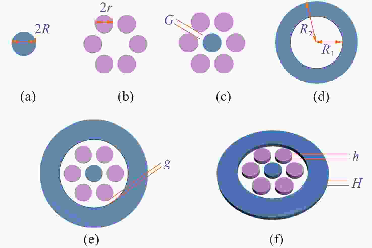
图 1 纳米环-七聚体金属-介电复合结构示意图。(a)最内层硅圆柱结构;(b)中间层银圆柱结构;(c)单硅圆柱与六银柱组合体;(d)最外层硅介质圆环结构;复合结构的(e)二维模型和(f)三维模型
Figure 1. Schematic diagram of the nanoring- heptamer metal-dielectric composite structure. (a) Innermost layer with silicon cylinder structure; (b) intermediate layer with silver cylinder structure; (c) single silicon cylinder and six-silver cylinders combination; (d) outermost layer with silicon dielectric ring structure; (e) 2D model and (f) 3D model of the composite structure
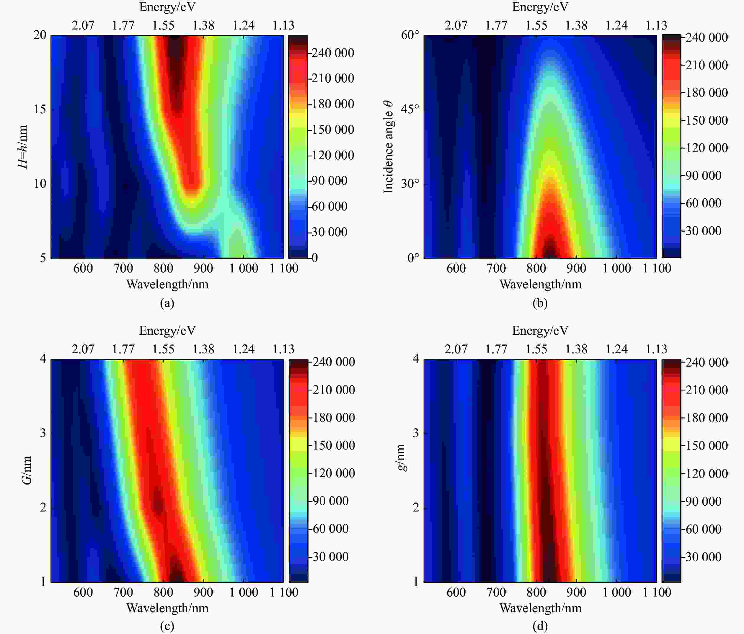
图 4 结构参数对散射谱线的影响示意图。(a)不同高度对散射强度及位置的影响;(b)不同入射角度对散射截面的贡献;(c)不同七圆柱间间隙对散射强度及位置的影响;(d)不同圆柱与圆环间隙对散射截面的贡献
Figure 4. Schematic diagram of the influence of structural parameters on scattering spectral line. (a) Influence of different height on scattering intensity and position; (b) contribution of different incidence angles to the scattering cross section; (c) influence of different gaps between seven cylinders on scattering intensity and position; (d) contribution of different cylindrical and annular gaps to the scattering cross-section
表 1 Sensitivity (S) of nanostructures changes with different materials
Table 1. Sensitivity (S) of nanostructures changes with different materials
First peak
(nm/RIU)Second peak
(nm/RIU)Third peak
(nm/RIU)n=1.02 800 750 1400 n=1.04 0 350 700 n=1.06 550 400 700 n=1.08 250 450 0 n=1.10 300 400 700 表 2 Figure of Merit (FOM) changes with different materials
Table 2. Figure of Merit (FOM) changes with different materials
First peak
(RIU−1)Second peak
(RIU−1)Third peak
(RIU−1)n=1.02 1.5 17 10.1 n=1.04 0 8.1 6.1 n=1.06 8.4 9 6.6 n=1.08 4.1 10.1 0 n=1.10 7 9.2 4.5 -
[1] ZHELUDEV N I. What diffraction limit?[J]. Nature Materials, 2008, 7(6): 420-422. doi: 10.1038/nmat2163 [2] SONG M K, MA Y P, LIU H, et al. High resolution of plasmonic resonance scattering imaging with deep learning[J]. Analytical Chemistry, 2022, 94(11): 4610-4616. doi: 10.1021/acs.analchem.1c04330 [3] GRAMOTNEV D K, BOZHEVOLNYI S I. Plasmonics beyond the diffraction limit[J]. Nature Photonics, 2010, 4(2): 83-91. doi: 10.1038/nphoton.2009.282 [4] FRISCHWASSER K, COHEN K, TSESSES S, et al. Nonlinear forced response of plasmonic nanostructures[J]. Physical Review Letters, 2022, 128(10): 103901. doi: 10.1103/PhysRevLett.128.103901 [5] LIU W, HU CH J, ZHOU L, et al. A square-lattice D-shaped photonic crystal fiber sensor based on SPR to detect analytes with large refractive indexes[J]. Physica E:Low-dimensional Systems and Nanostructures, 2022, 138: 115106. doi: 10.1016/j.physe.2021.115106 [6] WELFORD K. Surface plasmon-polaritons and their uses[J]. Optical and Quantum Electronics, 1991, 23(1): 1-27. doi: 10.1007/BF00619516 [7] LIU W, SHI Y, YI Z, et al. Surface plasmon resonance chemical sensor composed of a microstructured optical fiber for the detection of an ultra-wide refractive index range and gas-liquid pollutants[J]. Optics Express, 2021, 29(25): 40734-40747. doi: 10.1364/OE.444323 [8] LIU W, HU CH J, ZHOU L, et al. A highly sensitive D-type photonic crystal fiber infrared sensor with indium tin oxide based on surface plasmon resonance[J]. Modern Physics Letters B, 2022, 36(1): 2150499. doi: 10.1142/S0217984921504996 [9] LIMONOV M F, RYBIN M V, PODDUBNY A N, et al. Fano resonances in photonics[J]. Nature Photonics, 2017, 11(9): 543-554. doi: 10.1038/nphoton.2017.142 [10] ZHANG Y T. Photon-assisted Fano resonance tunneling periodic double-well potential characteristics[J]. Chinese Optics, 2021, 14(5): 1251-1258. doi: 10.37188/CO.2020-0068 [11] LUO L N, WANG Y K, NIE J Y, et al. Fano resonance properties of the arrays of metallic half-ring/rectangle structure[J]. Chinese Optics, 2015, 8(3): 360-367. doi: 10.3788/co.20150803.0360 [12] HOSSAIN M K, DRMOSH Q A. Silver nanoparticles and nanorings for surface-enhanced Raman scattering[J]. Plasmonics, 2022, 17(3): 1051-1064. doi: 10.1007/s11468-021-01572-w [13] ZHANG R X, DU CH L, SUN L, et al. Individual split au square nanorings for surface-enhanced Raman and hyper-Raman scattering[J]. Plasmonics, 2022, 17(3): 965-971. doi: 10.1007/s11468-021-01582-8 [14] RAZAVI Z, PAKARZADEH H. Third-harmonic generation in optical nanoantennas: efficiency enhancement[J]. The European Physical Journal Plus, 2022, 137(2): 183. doi: 10.1140/epjp/s13360-022-02378-3 [15] ALTUG H, OH S H, MAIER S A, et al. Advances and applications of nanophotonic biosensors[J]. Nature Nanotechnology, 2022, 17(1): 5-16. doi: 10.1038/s41565-021-01045-5 [16] BEUTLER H. Über Absorptionsserien von Argon, Krypton und Xenon zu Termen zwischen den beiden Ionisierungsgrenzen2 $ P^{2/0}_3 $ und2$P^{2/0}_1 $ [J]. Z. Physik, 1935, 93(3): 177-196.[17] FANO U. Sullo spettro di assorbimento dei gas nobili presso il limite dello spettro d'arco[J]. Il Nuovo Cimento (1924-1942), 1935, 12(3): 154-161. [18] YE J, WEN F F, SOBHANI H, et al. Plasmonic nanoclusters: near field properties of the fano resonance interrogated with SERS[J]. Nano Letters, 2012, 12(3): 1660-1667. doi: 10.1021/nl3000453 [19] YANG Q L, ZHANG X F, LIU F SH, et al. Multiple Fano resonances in gold split ring disk dimers[J]. Acta Physics Sinica, 2022, 71(2): 027802. (in Chinese) doi: 10.7498/aps.71.20210855 [20] YORULMAZ M, HOGGARD A, ZHAO H Q, et al. Absorption Spectroscopy of an Individual Fano Cluster[J]. Nano Letters, 2016, 16(10): 6497-6503. doi: 10.1021/acs.nanolett.6b03080 [21] ZHENG J D, LU H, XUAN X, et al. Plasmonic Fano-like resonance in double-stacked graphene nanostrip arrays[J]. Journal of the Optical Society of America B, 2022, 39(3): 843-850. doi: 10.1364/JOSAB.449405 [22] YANG L, WANG J CH, YANG L ZH, et al. Characteristics of multiple Fano resonances in waveguide-coupled surface plasmon resonance sensors based on waveguide theory[J]. Scientific Reports, 2018, 8(1): 2560. doi: 10.1038/s41598-018-20952-7 [23] KONG Y, CAO J J, QIAN W CH, et al. Multiple fano resonance based optical refractive index sensor composed of micro-cavity and micro-structure[J]. IEEE Photonics Journal, 2018, 10(6): 6804410. [24] PALIK E D. Handbook of Optical Constants of Solids[M]. New York: Academic Press, 1985. [25] LV J W, MU H W, LIU Q, et al. Multi-wavelength unidirectional forward scattering in the visible range in an all-dielectric silicon hollow nanodisk[J]. Applied Optics, 2018, 57(17): 4771-4776. doi: 10.1364/AO.57.004771 [26] ROCCO D, LAMPRIANIDIS A, MIROSHNICHENKO A E, et al. Giant electric and magnetic Purcell factor in dielectric oligomers[J]. Journal of the Optical Society of America B, 2020, 37(9): 2738-2744. doi: 10.1364/JOSAB.399665 [27] DENG Q R, CHEN J F, LONG L, et al. Silicon cuboid nanoantenna with simultaneous large Purcell factor for electric dipole, magnetic dipole and electric quadrupole emission[J]. Opto-Electronic Advances, 2022, 5(2): 210024. doi: 10.29026/oea.2022.210024 [28] LIU Q, JIANG Y, HU CH J, et al. High-sensitivity surface plasmon resonance sensor based on the ten-fold eccentric core quasi-D-shaped photonic quasi-crystal fiber coated with indium tin oxide[J]. Chinese Optics, 2022, 15(1): 101-110. doi: 10.37188/CO.EN.2021-0006 [29] BAZGIR M, JALALPOUR M, ZARRABI F B, et al. Design of an optical switch and sensor based on a MIM coupled waveguide using a DNA composite[J]. Journal of Electronic Materials, 2020, 49(3): 2173-2178. doi: 10.1007/s11664-019-07902-3 [30] GHODSI F, DASHTI H, AHMADI-SHOKOUH J. Design of a multilayer nano-antenna as a hyperbolic metamaterial with Fano response for optical sensing[J]. Optical and Quantum Electronics, 2020, 52(6): 316. doi: 10.1007/s11082-020-02431-4 -


 下载:
下载:


