


 HTML全文
 PDF 3898KB
金宝搏188软件怎么用 诱导击穿光谱技术(Laser-Induced Breakdown Spectroscopy,LIBS)是利用强脉冲金宝搏188软件怎么用 与物质相互作用所产生的等离子体光谱来实现对物质组成元素定性和定量分析的一种新方法。在脉冲金宝搏188软件怎么用 诱导等离子体的过程中,不同的金宝搏188软件怎么用 参数(能量、脉宽、波长)、检测过程中的环境条件以及材料本身的特性等,对金宝搏188软件怎么用 诱导等离子体的物理机制都有不同程度的影响,进而影响LIBS定量分析的结果。本文综述了现阶段LIBS技术中涉及的物理机制,包括LIBS基本原理、金宝搏188软件怎么用 参数区别、环境和材料特性差异所涉及的物理机制。为深入理解金宝搏188软件怎么用 与物质相互作用、提升LIBS检测能力提供了依据。

痕量气体作为大气的重要成份,对地球的生态起着重要作用。为了实现全天时连续测量、宽波段、高光谱的探测需求,本文设计了一款在掩星探测模式下工作的高光谱成像光谱仪。该系统为共狭缝的双通道结构,紫外-可见光通道采用单凹面光栅结构、红外通道采用利特罗与浸没光栅结合结构,有效地减小了体积。利用软件对光学结构进行优化,优化结果表明:光谱仪在250~952 nm波段范围内工作,其中紫外-可见光通道工作波段为250~675 nm、光谱分辨率优于1 nm、MTF在奈奎斯特频率为20 lp/mm处均高于0.58、全视场各波长处RMS值均小于21 μm;红外通道工作波段为756~952 nm、光谱分辨率优于0.2 nm、MTF在奈奎斯特频率为20 lp/mm处均高于0.76、全视场各波长处RMS值均小于6 μm,均满足设计要求,该高光谱成像光谱仪系统可以实现对痕量气体的掩星探测。

针对彩色数字相机高成像质量以及高色准的需求,本文研究了基于Philips棱镜的3CMOS相机的光学系统设计以及相机光谱优化方法。通过对Philips棱镜进行光路建模的方法优化了棱镜的结构参数,使棱镜在保证全内反射以及出射窗口大小的条件下,减小了系统的体积,并由此设计了Philips棱镜3CMOS相机光学系统,其视场角为45°,相对孔径1/2.8,系统的MTF在110 lp/mm的奈奎斯特采样频率下全视场全波段均大于0.4。之后,基于色度学基本原理建立了Philips棱镜相机的矢量成像模型,分析了由光线入射角度的变化造成的薄膜光谱偏移问题,提出了宽光束下光谱偏移的修正模型。利用该模型设计并优化了相机中的四组光学薄膜,通过光路仿真实验以及色差分析,基于优化后的相机光谱,系统的平均色差降低了15.8%,像面颜色不均匀性降低了60%。结果表明:本文设计的光学系统拥有良好的成像质量,并且优化后的相机光谱实现了良好的颜色性能以及颜色均匀性。

太赫兹波具有高穿透性、低能性及指纹谱性等特征,在探测领域被广泛应用,因此设计太赫兹波成像光学系统具有重要的意义和广泛的应用前景。首先,以四块透镜构成的天塞物镜为参考结构,应用近轴光学系统像差理论构建系统像差平衡方程,给出了系统初始结构参数求解函数和方法,再结合光学设计软件对系统像差进一步校正,最终设计了一种用于太赫兹波探测的大孔径光学成像系统。该光学系统由四块同轴折射透镜构成,焦距70 mm,F数为1.4,全视场角为8°,在奈奎斯特频率10 lp/mm处全视场角范围内的调制传递函数(MTF)值均大于0.32,各视场内的弥散斑均方根(RMS)半径均小于艾里斑半径,最后对系统各种公差进行分析和讨论。设计结果表明,本文设计的太赫兹波探测光学成像系统具有孔径大、结构简单且紧凑、成像质量较好且加工性易于实现等特点,满足设计要求,它在太赫兹波段高分辨率探测领域具有重要应用价值。

鬼像是由于镜面间的残余反射所产生的一种杂散光。鬼像会降低光学系统的成像清晰度,湮灭目标,严重影响光学系统的性能。为了探究鬼像对成像系统性能的影响,构建了二次反射产生的鬼像影响下的调制传递函数(MTF)的计算模型。本文首先介绍了在近轴近似下的鬼像分析与描述的方法。接着,从调制传递函数的定义出发,考虑鬼像在像面处的照度对像面调制度的影响,构建了鬼像影响下的MTF计算模型。通过对一系统进行实例计算,并与仿真结果进行比对得到均方误差最大不超过0.049373,进而验证了该模型的准确性。同时针对误差较大的结果进行了详细分析,明确了该计算方法的适用范围。研究结果表明,利用近轴近似的方法计算鬼像影响下的MTF在大多数情况下是真实准确的,该研究为光学系统的鬼像分析方面做出了有益探索。


液晶波前校正器通常基于液晶显示器的工艺制备而成,因此其研制成本高、定制难度大。本文基于掩模光刻法制备液晶波前校正器,以实现液晶波前校正器的专用化、低成本研制。首先,基于掩模光刻技术设计并制备了91像素的无源液晶驱动电极,并封装成液晶光学校正单元。然后,设计并制备了驱动连接电路板,实现液晶光学驱动单元和驱动电路板的匹配对接。接着,进行液晶波前校正器响应特性检测,结果显示,其相位调制量为5.5个波长,响应时间为224 ms。最后,利用Zygo干涉仪进行球面波的产生和静态倾斜像差的校正,结果显示,其可以产生正负离焦波前,且对水平倾斜像差校正后,Zernike多项式中第一项的值从1.18降至0.16,校正幅度达86%,实现了像差的有效校正。本文的研究工作可为液晶波前校正器的研制提供新思路,进而拓宽其应用领域和场景。

点云配准是获取三维点云模型空间姿态的关键步骤,为了进一步提高点云配准的效率和准确性,提出了一种基于逐点前进法特征点提取的改进型点云配准方法。首先,利用逐点前进法快速提取点云特征点,在保留点云模型特征的同时大幅精简点云数量。然后,通过使用法向量约束改进的KN-4PCS算法进行粗配准,以实现源点云与目标点云的初步配准。最后,使用双向Kd-tree优化的LM-ICP算法完成精配准。实验结果表明,本文方法具有较高的精度和效率,同时具有较好的鲁棒性,在斯坦福大学开放点云数据配准实验中,其平均误差较SAC-IA+ICP算法减少了约70.2%,较NDT+ICP算法减少了约49.6%,配准耗时分别减少约86.2%和81.9%,同时在引入不同程度的高斯噪声后仍能保持较高的精度和较低的耗时。在真实室内物体点云配准实验中,其平均配准误差为0.0742 mm,算法耗时平均为0.572 s。通过斯坦福开放数据与真实室内场景物体点云数据对比分析表明,本方法能够有效地提高点云配准的效率、准确性和鲁棒性,为基于点云的室内目标识别与位姿估计奠定了良好的基础。

针对高能金宝搏188软件怎么用
器出光过程中出现的大量离焦和0°像散低阶像差这一现象,提出了基于哈特曼波前传感器和二维整形光路的XY离焦像差校正方法。首先通过对Zernike多项式的离焦项和0°像散项进行线性组合得到XY离焦像差表达式,该XY离焦像差系数大小可直接表征X离焦和Y离焦的波前PV值。同时,通过微调高能金宝搏188软件怎么用
器中二维整形光路中的镜子间距,可实现金宝搏188软件怎么用
器输出光束XY离焦波面的补偿。因此,首先利用哈特曼波前传感器提取出光束的XY离焦像差系数大小,而后计算机再根据XY离焦像差系数大小实时闭环微调二维整形光路中的镜子间距,从而实现XY离焦像差的校正,改善输出光束的光束质量。实验结果表明,该方法可有效地将高能金宝搏188软件怎么用
器输出光束XY离焦量的PV值由5.2 μm和1.1 μm校正到0.5 μm以下,相应的光束质量

三维重构是文物数字化的关键技术,其中三维点云配准精度是评估重构质量优劣的重要指标之一。实际采样中,文物点云细节信息繁多,传统降采样后易出现细节缺失从而影响配准精度。为了解决这一问题,本文提出了一种基于曲率特征的文物点云分类降采样与配准方法。首先,通过线性矩阵金宝搏188软件怎么用 测量获取文物的三维点云数据。其次,计算所有点的曲率值,并设置曲率阈值进行点云分类,不同点集按照其特征属性进行不同权重的降采样,从而最大限度地保留点云的形态特征和细节信息。最后通过求解刚性变换模型实现点云的配准。点云配准前的降采样处理后点云数据降至原始点云的1/3,与传统的整体降采样ICP方法对比,平均距离从0.89 mm约降至0.59 mm,标准偏差从0.29 mm约降至0.18 mm。在降低点云数据的同时也保证了配准的精度,适用于不同类型的文物点云数据。

为解决相位生成载波-反正切解调算法(PGC-Atan)的非线性失真问题,搭建了基于改进型PGC-Atan算法的非本征型法珀传感器(EFPI)解调系统。首先,理论分析载波相位调制深度(C)偏离最优值、伴生调幅、载波相位延迟等非线性因素对经典PGC-Atan算法中参与反正切运算的正弦与余弦两路信号的影响。然后,针对外调制或伴生调幅较小的情况,提出了一种基于系数补偿的改进型PGC-Atan算法(PGC-CC-Atan)。该算法通过构造与C值和载波相位延迟有关的系数,消除反正切运算中的非线性参数。针对内调制情况,提出了一种基于椭圆拟合的改进型PGC-Atan算法(PGC-EF-Atan)。该算法通过基于分块矩阵的最小二乘法拟合椭圆并提取3个椭圆参数,进而将受非线性因素影响的正弦与余弦两路信号校正为正交信号。最后,通过仿真验证了改进型算法的正确性,并采用高调制特性的垂直腔面发射金宝搏188软件怎么用 器(VCSEL)和常规腔长的EFPI传感器等搭建PGC解调系统,对比经典PGC-Atan算法与两种改进型算法的解调性能,证实了改进型算法抑制非线性失真的有效性。实验结果表明:一定C值范围内,两种改进型算法可在非线性因素影响下有效解调。PGC-EF-Atan算法相较于PGC-CC-Atan算法,解调信纳比提升了11.602 dB,总谐波失真降低了10.951%。两种改进型算法中,PGC-EF-Atan算法对非线性失真的抑制效果更好,且解调线性度良好,准确度高。

针对传统单目视觉测量系统测量视场有限的问题,本文提出一种基于双自由度旋转平台的全向空间单目视觉测量方法。首先,对双自由度旋转平台的转轴参数进行标定,用副相机拍摄与双自由度转台固定的棋盘格标定板,对棋盘格角点的位置坐标进行提取并转化到同一相机坐标系下;利用PCA(主成分分析)平面拟合得到初始位置转轴参数中的方向向量,通过使用空间最小二乘圆拟合的方法,得到初始位置时转轴参数中的位置参数;然后,通过转台转动的角度以及罗德里格斯公式将不同位置下相机获取的数据进行坐标系统一,实现水平和竖直方向全向空间下的目标测量;最后,通过高精度金宝搏188软件怎么用 测距仪验证了本方法的测量精度,并通过与双目视觉测量系统、wMPS测量系统进行比对实验,验证了本方法的全向空间测量能力。实验结果表明,本方法测量精度基本达到双目视觉测量系统水平,但测量范围远大于双目视觉测量,可以满足全向空间测量要求。

为了提高柔性机器人抓握传感中掌心表面的重构精度,本文基于COMSOL仿真,在436 mm×436 mm×2 mm聚丙烯板上,采用7只经聚二甲基硅氧烷(PDMS)封装的光纤光栅(FBG)柔性传感器,选取环形布设的方式,在板末端中心与两角分别受力的情况下,使用光纤光栅解调仪采集实验中的传感器数据,并通过三次样条插值法进行连续化,设定数个平面Y与拟合圆环相交,计算过点函数获得三维曲面点集,实现了空间曲面的拟合可视化显示。在曲面末端中心受力时,板末端位移最小相对误差为0.549%,最大相对误差为8.300%,最小绝对误差为0.051 cm,最大绝对误差为1.255 cm,板末端两角受力时,板面重构末端位移最小相对误差为2.546%,最大相对误差为14.289%,最小绝对误差为0.005 cm,最大绝对误差为0.729 cm。实验结果为柔性机器人掌心抓握传感提供了应用基础。

为了实现凹非球面的快速、高精度与通用化检测,文中提出了一种将非球面当做球面直接采用干涉仪检测的非零位干涉检测方法,并结合相应的数据处理方法,获得非球面的面形误差检测结果。首先介绍了该方法的检测原理,建立了回程误差、调整误差的计算与去除模型,研究了面形误差的数据处理方法。然后以两个不同非球面度的凹非球面为例,对其回程误差和调整误差进行了仿真计算,验证了该方法的有效性。最后搭建了凹非球面的非零位检测实验装置,成功测量得到其面形误差。通过与自准直零位检测法及LUPHOScan轮廓测量法检测结果的对比,发现两种方法测量得到的误差结果的面形分布和评价指标具有高度一致性,验证了该检测方法的正确性。该检测方法在保证高精度测量的同时兼备一定的通用性与便捷性,为凹非球面的通用化检测提供了一种有效手段。

针对现有多波段成像系统体积大、功耗高和集成化设计困难的问题,本文提出了一种基于单传感器的三波段共口径成像光学系统的设计方法。首先,在光学系统的光阑处设计1×2多波段透镜阵列,把可见光波段和短波红外波段同时成像在一个像平面上,并把两个波段中心波长的成像位置偏差控制在一个像元内以实现双波段融合成像。然后,针对双波段成像衍射极限不同的问题,提出分通道透镜阵列的离轴偏移量和通光口径大小联合优化的方法,并采用双电动光阑高速控制三个成像通道的切换速度。最后,设计了一个基于单传感器的焦距为30 mm,工作波段分别为480~900 nm、900~1700 nm和480~1700 nm的三波段共口径光学系统,设计及分析结果表明该系统具有成像质量好、结构紧凑、无运动光学元件、成像波段切换速度快等优点。

为了解决在光声层析成像(photo acoustic tomography,PAT)中,由于不均匀光通量分布、组织复杂的光学和声学特性以及超声探测器的非理想特性等因素所致的重建图像质量下降的问题。本文提出一种PAT图像重建方法,建立考虑不均匀光通量、非定常声速、超声探测器的空间脉冲响应和电脉冲响应、有限角度扫描和稀疏采样等因素的前向成像模型,通过交替优化求解成像模型的逆问题,实现光吸收能量分布图和声速分布图的同时重建。仿真、仿体和在体实验结果表明,与反投影法、时间反演法和短滞后空间相干法相比,该方法重建图像的结构相似度和峰值信噪比可分别提高约83%、56%、22%和80%、68%、58%。与传统方法相比,对非理想成像场景采用该方法重建的图像质量有显著提高。

为了研制高灵敏海水盐度传感器,本文基于CO2金宝搏188软件怎么用 技术成功制备出一种工作在色散转折点(DTP)附近的长周期光纤光栅(LPFG)。首先,利用CO2金宝搏188软件怎么用 器在80 μm细单模光纤上制备出工作在DTP附近的LPFG,证明了采用CO2金宝搏188软件怎么用 微加工技术制备较短周期LPFG的可能性。其次,通过调控CO2金宝搏188软件怎么用 器的制备周期,使高阶包层模式LP1,9工作在DTP附近,从而显著提高了LPFG的折射率灵敏度。在双峰谐振增敏效应的作用下,当海水盐度从5.001 ‰变化到39.996 ‰时,光栅周期为115.4 μm的双峰谐振LPFG平均灵敏度高达0.279 nm/‰。研究结果表明,本文制备的LPFG海水盐度传感器具有谐振损耗大和灵敏度高的优点,其在海水盐度监测领域具有较好的应用前景。

为了降低探测器的噪声与暗电流,使光谱仪的CMOS探测器获得更准确的光谱曲线,设计了探测器温度控制系统。本系统核心采用基于现场可编程逻辑门阵列(FPGA)的增量式比例-积分-微分(PID)控制算法。在传统控制算法的基础上,增加了抗积分饱和控制,并且在PID算法的前端增加了对目标值的过渡过程,实现探测器温度变化速率可控的同时,也解决了超调过大的问题。多次整机环境实验表明,在轨环境温度条件下、40 °C温差范围内,系统可以控制探测器以指定温变速率4.5±0.05 °C/min达到任意温度,并且在该温度下稳定工作,温度变化范围为±0.1 °C。相比于传统模拟PID控制方法,具有灵活度高,稳定性强等优点。制冷到−10 °C时,探测器的噪声得到了有效的抑制。

本研究分析了目前用于显示器的高均匀宽角度灯珠的光学要求。采用新型非朗伯(non-Lambertian)分布封装Micro-LED芯片,实现了宽光束、高均匀性的微型LED芯片光珠。本文分析了在不同封装倾角、封装高度、封装材料、封装支架材料、蓝宝石厚度和图案化蓝宝石衬底尺寸下,使用由不同封装材料(铜、钛、铝和银)和材料类型(完全反射和完全吸收)组成的支架,模拟了固定灯珠的光输出效率和出光角度的变化。通过调整材料、芯片和封装参数,本文看可以得到一个、两个或三个光束,具有贴片灯珠的宽角度、高均匀性的远场光分布特性,可以满足当前LED和LCD的显示要求。

为了提高可见光波段(0.3 μm~0.9 μm)高温标定的效率,提出了可见光波段高温标定的简化方法。首先,提出了带有曝光时间变量的可见光波段的高温标定模型,通过大量的实验数据发现,RGB相机各个通道的灰度值不仅随曝光时间递增呈线性变化,且随黑体辐射亮度递增呈线性变化,进而确定了可见光波段高温标定模型的具体形式。然后,为了求解简化后的可见光波段高温标定模型中的未知数,在两个黑体辐射亮度下,分别采集两个曝光时间下的图像数据,接着,对图像数据进行处理,便可以得到任意曝光时间下的RGB相机高温标定曲线。最后,对本文提出的简化可见光波段高温标定方法与常规按曝光时间进行可见光波段高温标定法进行比较。实验结果表明:R通道计算值与标定值的相对误差最大值为3.38%、G通道计算值与标定值的相对误差最大值为2.56%、B通道计算值与标定值的相对误差最大值为−1.14%,且各通道的计算值与标定值的相对误差均未超过3.50%。本文提出的数学模型可以有效地简化传统的高温标定法,进而大大的缩短了高温标定时间,提高了高温标定的标定效率。

为缩短12寸晶圆检测成像系统的轴向和径向尺寸,提出一种小角度棱镜折转光路与超短物像距镜头相结合的解决方法。设计优于1/12λ(λ=632.8 nm)面形精度的小角度棱镜折转光路,实现照明系统与成像镜头的水平布置,径向尺寸仅为80 mm,在保证不影响系统成像质量的前提下,极大降低整个系统径向尺寸;同时也实现12°的小角度明场照明。设计放大倍率为0.264的对称混合型光学系统,采用纯球面系统获得较大成像视场,像高81.92 mm,物像距仅为392.5 mm,极大降低整个系统轴向尺寸。设计结果表明,整个成像系统全视场平均光学传递函数优于0.4@100l p/mm,相对畸变优于0.03%,像面照度均匀性全视场优于50%。实际测试结果表明,全视场实际成像分辨率优于18.88 μm,达到了系统极限分辨率;全视场像面照度均匀性为43.3%,满足均匀性优于40%的研制要求。研究结果表明,提出的超薄超短物像距高分辨率检测成像系统合理、有效,解决了12寸晶圆检测成像系统空间尺寸压缩的难题,并降低了研制成本,为后续近距离大尺寸物体检测成像系统的研制提供参考依据。

相较于单涡旋光束,涡旋阵列光束能够扩充信息的传输容量,研究其传输特性对其光通信应用具有重要意义。本文选取阶数为

小尺寸零件的表面积小、结构复杂,传统标志点拼接方法需要在零件表面人工粘贴标志点,导致表面的测量数据缺失成为孔洞;基于特征的点云拼接方法要求零件表面具有易区分的几何或距离特征,不适用于包含重复性特征的回转体零件。本文提出一种基于机械拼接的无标志点扫描测量方法,不需要粘贴标志点,不依赖于零件表面特征。首先,采用基于摄影测量的相机标定方法重建标定板上靶点的高精度三维坐标,通过跟踪编码靶点的位置建立转台不同转角对应的旋转矩阵,进而解算出转轴方向向量和轴上定点坐标,实现转轴和相机的同步标定。其次,在完成两个转轴位姿精确标定的基础上,利用转台转角构建旋转拼接矩阵,实现多视角点云粗配准。最后,基于法向迭代最近点算法(Normal Iterative Closest Point, NICP)完成点云的精配准。实验结果表明:使用靶点跟踪法标定后的两转轴夹角误差较传统的标准球拟合法低0.023°,标定后测量标准球的整体平均尺寸误差小于0.012 mm;在小尺寸零件自动化测量时,机械拼接方法在精配准后的点云拼接效果与标志点拼接方法相近,且拼接稳定性更高。机械拼接方法适用于无法粘贴标记点的小尺寸零件三维形貌测量场景。

随着制冷型长波红外焦平面探测器空间分辨率及面阵规格的提升,制冷型长波红外热像仪应用范围越来越广,需提升相应光学系统以满足不同领域需求。长波红外变焦光学系统相对于中波红外变焦光学系统存在可用材料少、系统高低温环境无热化难度大等难题。本文采用机械补偿变焦技术实现光学多视场变焦,利用主动补偿的消热差技术达到系统在−40 °C~+65 °C温度范围成像清晰,实现四片透镜架构的制冷型长波红外四视场光学系统设计。该光学系统四视场焦距分别为25 mm、109 mm、275 mm、400 mm,变倍比为15.0×,光学系统包络尺寸为268 mm(长)×200 mm(宽),光学零件总质量618 g。该光学系统具有质量轻、性能高、成本低等SWaP-C特征,将在辅助导航、搜索、跟踪等安防领域中得到广泛应用。

随着星间通信系统的迅速发展,数据传输的精度要求不断提高。分光镜作为系统的核心元件,其光谱特性和面形精度直接影响整个系统的传输精度。本文基于薄膜干涉理论,选取Ta2O5与SiO2作为高低折射率膜层材料进行膜系设计,采用电子束蒸发的方式在石英基板上制备高精度分光镜。同时根据膜层应力补偿原理建立面形修正模型,修正分光镜面形。经光谱分析仪检测,分光镜在入射角度为21.5°~23.5°范围内,1563 nm透过率大于98%,1540 nm反射率大于99%。经金宝搏188软件怎么用 干涉仪检测,分光镜反射面形精度RMS由λ/10修正至λ/90(λ=632.8 nm),透过面形精度RMS为λ/90。

明场成像能够提供细胞或组织的形态学信息,荧光成像可以获取关键蛋白的表达信息,基于两者的双模态关联成像是目前医学和科研中常用的组织样本检查方式。然而,在临床检查时通常利用基于邻近切片之间的关联成像进行观察。此时,组织结构和细胞层次均会有或多或少的改变,这在样本量不足、切片上的细胞有限或需要获得点对点精准形态学信息的情景下显得十分不利。因此,发展单切片双模态光学关联成像技术,在单张切片上同时提供组织形态和多个目标蛋白的分布及表达,有助于更准确地描述肿瘤及其微环境。在样本量稀缺的肾脏病理检测中,该技术显得尤为重要:肾脏病理需要利用明场成像获取苏木素-伊红染色后组织和细胞的病理形态学信息,而利用荧光成像来获取多个目标蛋白的分布及表达情况则是肾脏免疫病理筛查的必检分子项目。本文重点研究了将苏木素-伊红染色和免疫荧光染色在同一张肾脏切片上实现的组织样本处理方法,对染色、褪色及复染的流程进行改良和效果对比,并探索将单切片双模态图像进行创新性融合。

生物组织散射引起的光学像差限制了光学系统的成像性能。本文研究了基于间接波前整形的近红外二区荧光共聚焦成像技术。首先,合成制备了高效率近红外二区荧光探针,在该波段生物组织散射的降低有助于实现高对比度的活体组织成像。其次,研究了基于间接波前测量的自适应光学办法,将间接波前整形技术应用于金宝搏188软件怎么用 扫描共聚焦显微系统中,以实现对于生物组织引起的光学像差的测量与补偿,获得生物组织的高信噪比成像。最后,对基于间接波前整形的近红外二区荧光共聚焦成像系统开展了相关实验。实验结果表明,本系统对空气平板、散射介质和小鼠颅骨等产生的像差具有良好的补偿效果,分别将最终信号强度提升为1.47、1.95和2.85倍,显著提升了最终的成像质量。

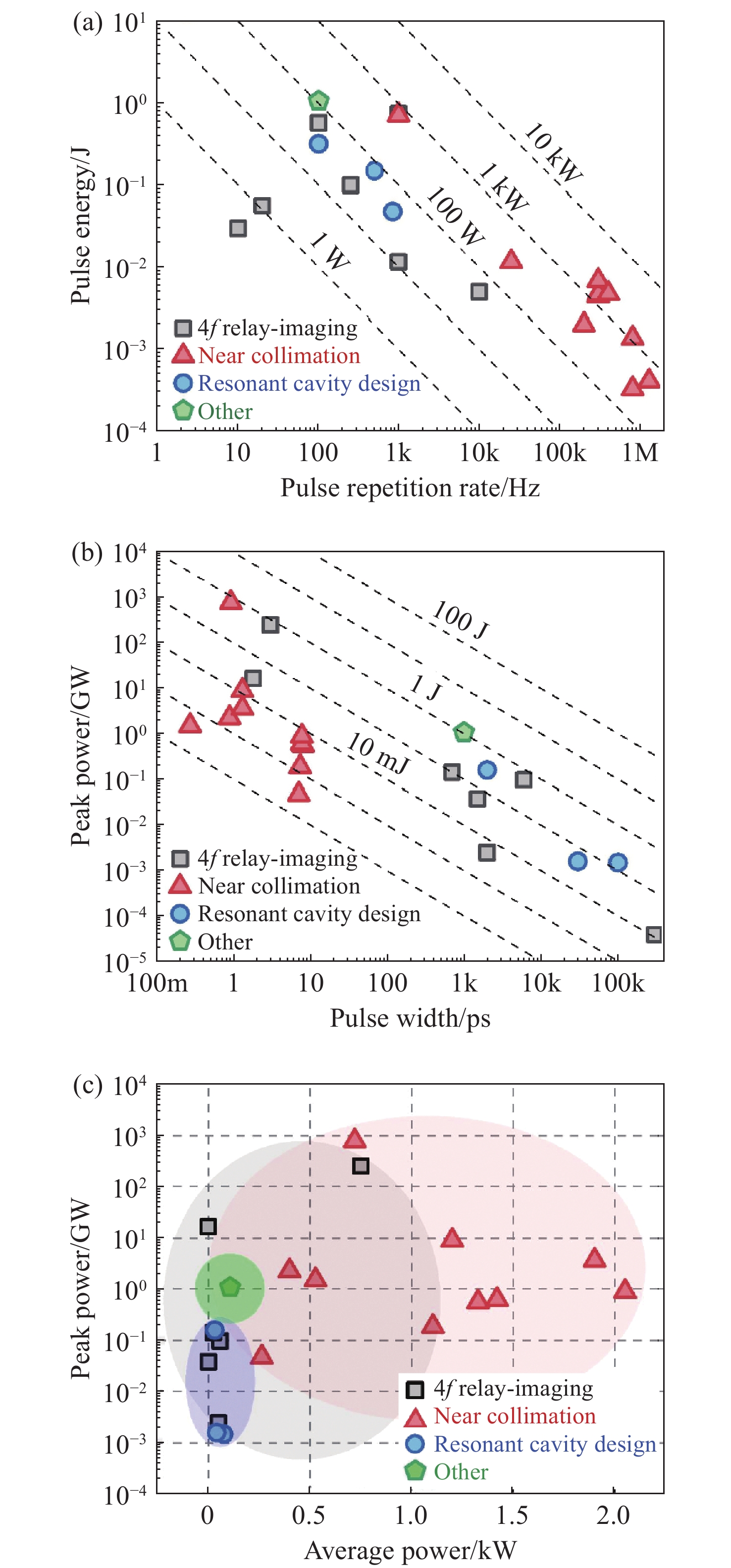
基于多纵模振荡种子源的窄线宽光纤金宝搏188软件怎么用 器具有光路简单、结构紧凑、可靠性高、成本低等特点,在实际工程应用以及在空间受限的载荷平台上有着显著优势,是高功率光谱合成的理想子束模块。受自脉冲效应的影响,多纵模振荡种子源的时域特性较差,导致了放大过程中产生较强的光谱展宽与受激拉曼散射效应,这限制了输出功率的进一步提升并降低了其光谱纯度。本文首先介绍了四种常见的窄线宽种子源,并重点分析了多纵模振荡种子源中自脉冲效应的产生机理及抑制方法,对优化多纵模振荡种子源和放大器的关键技术进行了详细介绍,归纳总结了近几年的技术突破与研究成果,对未来的发展方向进行了展望分析,为基于多纵模振荡种子源的窄线宽金宝搏188软件怎么用 器的功率提升和光谱优化提供一定思路。

遥感卫星在国防和民用探测等领域发挥着重要作用,而大气湍流严重影响高分辨率遥感卫星的成像质量。本文重点研究遥感卫星对地探测时,相机口径、卫星轨高和大气湍流强度对空间相机成像质量的影响。首先基于球面波传输模型和Kolmogorov湍流理论,对空对地探测湍流波前进行仿真;然后分析畸变波前随相机口径、卫星轨高和大气相干长度的变化规律,推导出普适公式,并进一步推导出空间相机成像分辨率随相机口径、卫星轨高和大气相干长度变化的计算公式;最后,研究了大气湍流对空间相机调制传递函数(MTF)的影响,并以MTF=0.15为基准,仿真分析了MTF相对误差随相机口径、卫星轨高和大气相干长度的变化规律。本研究为高分辨率遥感卫星的设计、分析和评估提供理论依据。

随着工业制造不断向智能化、精密化、集成化方向发展,对加工过程进行在机检测,可及时反馈测量结果并补偿修正加工参数,有助于提高加工精度和效率。条纹结构光技术是近年来发展迅速的非接触式测量方法,具有测量原理简单、成本低、测量精度高、易于集成等特点,为在机检测提供了新的解决方案。由于加工环境光线复杂且金属零件本身具有高反光的特性,造成结构光在机检测的精度降低,测量结果不准确,将高动态范围(High Dynamic Range, HDR)技术应用于结构光检测中,可实现对金属零件在复杂场景的测量,抑制高反光的影响。本文首先介绍了结构光测量原理,总结出HDR结构光在机检测面临的难点;其次,对HDR结构光技术进行了全面综述,以机械加工在机检测为背景,按照基于硬件设备的HDR技术和基于条纹算法的HDR技术分别进行了归纳分析;然后,根据在机检测的条件需求,对各类技术进行了总结,比较不同方法的优缺点和在机检测的适用性;最后,结合近年来先进制造技术和精密测量的研究热点,进行潜在应用分析,提出技术展望。

为提供高品质、智能健康的照明光源,基于三基色LED光源构建了线性调光混合照明系统,并提出一种调光调色的优化方法。混合光源的光色度和光强度分别用色温和明度等级来设定,使得混合照明效果更加符合“人因照明”的需求。在系统的智能优化配光过程中,将色温转化为CIE
为了满足国家同步辐射光源的需要,对单晶硅小闪耀角光栅的各向异性湿法刻蚀制备工艺展开了研究,制备适用于软X射线中波波段的闪耀光栅。首先基于严格耦合波法对小闪耀角光栅进行了结构参数优化及工艺容差分析。在晶向对准过程中,先通过环形预刻蚀确定硅片晶向,再基于倍频调整法实现光栅掩模与单晶硅<111>晶向的对准。同时研究了光刻胶灰化技术及活性剂对光栅槽形质量的影响,并通过单晶硅各向异性湿法刻蚀工艺成功制备了接近于理想锯齿槽形的闪耀光栅。实验结果证明:所制备光栅闪耀角为1°,刻线密度为1200 gr/mm,闪耀面均方根粗糙度在0.5 nm以内。此方法可以应用于软X射线中波波段闪耀光栅的制作,在获得较高衍射效率的同时可以大大减少其制作难度及成本。

相位提取与深度估计是结构光三维测量中的重点环节,目前使用传统方法对结构光进行分析存在效率不高、结果不够鲁棒等问题。为了提高结构光重建效果,本文提出了一种基于轻型自限制注意力(Light Self-Limited-Attention,LSLA)的结构光相位及深度估计混合网络,即构建了一种CNN-Transformer的混合模块,并将构建的混合模块放入U型架构中,实现了CNN与Transformer的优势互补。将所提出的网络在结构光相位估计和结构光深度估计两个任务上进行了实验,并和其他网络进行了对比。实验结果表明,相比其他网络,本文所提出的网络在相位估计和深度估计的细节处理上更加精细,在结构光相位估计实验中,精度最高提升31%;在结构光深度估计实验中,精度最高提升26%,提高了深度神经网络在结构光相位估计及深度估计的准确性。

视差不连续区域和重复纹理区域的误匹配率高一直是影响双目立体匹配测量精度的主要问题,为此,论文提出一种基于多特征融合的立体匹配算法。首先在代价计算阶段,通过高斯加权法赋予邻域像素点的权值,从而优化绝对差之和(Sum of absolute differences,SAD)算法的计算精度,并基于Census变换改进二进制链码方式,将邻域内像素的平均灰度值与梯度图像的灰度均值相融合,进而建立左右图像对应点的判断依据并优化其编码长度;然后,构建基于十字交叉法与改进的引导滤波器相融合的聚合方法,从而实现视差值再分配以减低误匹配率;最后,论文通过赢家通吃(Winner Take All,WTA)算法获取初始视差,并采用左右一致性检测方法、亚像素法提高匹配精度,从而获取其最终的视差结果,进而建立基于多特征SAD-Census变换的立体匹配算法。实验结果表明,在Middlebury数据集的测试中,所提算法的平均非遮挡区域和全部区域的误匹配率为分别为2.67%和5.69%,测量200−900 mm距离的平均误差小于2%;而实际三维测量的最大误差为1.5%。实验结果检验了论文所提算法的有效性和可靠性。

为了实现可见光波段多路不同波长金宝搏188软件怎么用 的周期性闭环校正,设计了一种具有光束指向和位置偏差独立监测与调节的金宝搏188软件怎么用 合束系统。首先,根据系统的应用需求,提出了合束系统的设计指标与整体合束方案。然后,在合束方案的基础上,建立了合束系统的光束控制模型,并通过数值仿真得到了合束系统光束控制的解算方法。闭环合束系统通过光束指向和位置监测装置分别实现合束金宝搏188软件怎么用 指向偏差与位置偏差的独立监测,并根据监测结果进行光束调节装置控制量的解算;进而通过两维摆镜和一维平移台分别实现光束指向和位置偏差的独立高效调节。最后,采用两路不同波长的金宝搏188软件怎么用 束,配合光束监测与调节装置,搭建了闭环合束模拟实验平台,对周期性闭环合束系统的合束效果进行了验证。实验结果表明:在长时间的工作过程中,两路金宝搏188软件怎么用 均实现了与基准光路的精密合束,合束指向精度优于±7 μrad,位置精度优于±0.84 mm。本研究所组建的金宝搏188软件怎么用 合束系统不仅具有合束精度高、校正速度快、光路扩展性强的优势,而且可实现金宝搏188软件怎么用 束的周期性闭环校正,能够有效保证合束金宝搏188软件怎么用 的长期工作稳定性。

细胞内镜需实现最大倍率约500倍的连续放大成像,受光纤照明及杂散光影响,其图像存在不均匀光照,且光照分布会随放大倍率而变化,这会影响医生对病灶的观察及判断。为此,本文提出一种基于细胞内镜光照模型的图像不均匀光照校正算法。根据图像信息由光照分量和反射分量组成的原理,该算法通过卷积神经网络学习图像的光照分量,并基于二维Gamma函数实现不均匀光照校正。实验表明,经本文方法进行不均匀光照校正后,图像的光照分量平均梯度和离散熵分别为0.22和7.89,优于自适应直方图均衡化、同态滤波和单尺度Retinex等传统方法以及基于深度学习的WSI-FCN算法。

 摘要(34)
Time of Flight(ToF)深度相机是获取三维点云数据的重要手段之一,但ToF深度相机受到自身硬件和外部环境的限制,其测量数据存在一定的误差。针对ToF深度相机的非系统误差,本文通过实验验证了被测目标的颜色、距离和相对运动均会对深度相机获取的数据产生影响,且所生的误差影响均不相同。基于摆动误差以及任何信号都可以表示成傅里叶级数的形式,文中提出了新的测量误差模型对颜色和距离产生的误差进行了校正;对于相对运动产生的误差,建立了三维运动模糊函数进行恢复。通过对所建的校正模型进行数值分析,距离和颜色的残余误差小于4 mm,相对运动所带来的误差小于0.7 mm。本文所做工作改善了ToF深度相机的测量数据的质量,为开展三维点云重建等工作提供了更精准的数据支持。

剪切散斑干涉是一种非接触式、全场高精度光学变形测量技术,由于环境等因素导致采集的散斑条纹图像存在大量随机噪声,进而影响测量精度。传统去噪方法在滤除噪声的同时,容易导致条纹边缘信息的丢失甚至破坏。针对该问题,本文提出基于正余弦变换和双调滤波相结合的剪切散斑干涉图像去噪方法。该方法首先对相位条纹图进行正余弦变换获得两幅图像,其次对这两幅图像分别运用双调滤波方法进行去噪,最后将滤波后的两幅图像合并为最终的相位条纹图。实验结果表明:经提出方法滤波后的相位图散斑抑制指数为0.999,平均保持指数为2.995,证明该方法较传统去噪方法更好地改善相位图质量,且能大程度保留相位条纹的细节及边缘信息。

智慧汽车的发展对具备投影功能的智能车灯系统提出了更高的要求。Micro LED投影显示技术因其良好的自发光特性使之与传统技术相比系统结构更为简单,光利用率更高,更有利于小型化、节能化和集成化。本文提出了一种基于Micro LED阵列的车灯投影方案,设计了以像素尺寸为80 μm×80 μm的200×150白光Micro LED阵列作为显示光源,视场角为16°×34°物像倾斜的车灯投影光学系统,对物面倾斜角度和光学系统结构进行了优化。此外,分别采用反向畸变处理方法和像素灰度调制方法解决车灯投影图像的梯形畸变和照度均匀性问题,并搭建了投影实验平台,对图像校正方法进行了验证。实验结果表明:校正后x、y方向的图像梯形畸变系数分别从0.0932和0.3680下降至0.0835和0.0373,像面照度均匀性从83.2%提高到93.2%。本文通过基于Micro LED的倾斜投影车灯光学系统优化设计及其图像校正方法,实现了高光效、低畸变的车灯投影。

随着低轨空间资源愈发拥挤,空间态势感知是太空资产正常运行的重要支撑,而光学观测是其重要手段之一。本文针对空间目标受到的太阳辐射、地球辐射、地球反照辐射,采用蒙特卡洛(Monte Carlo)法,基于非结构四面体网格编写了仿真程序,并对计算结果进行了对比验证。进一步地,对太阳同步轨道卫星受到的轨道外热流,采用带帆板的网格进行了有无遮挡情况下各表面受到的轨道外热流分析。结果显示,在对地模式下考虑遮挡后,-Y表面平均热流值降低了53.79 W/m2,+Y-Z侧帆板表面平均热流值降低了32.05 W/m2。结合表面材料属性,给出了各表面的温度特性,并结合帆板温度的在轨遥测数据,验证了计算的准确性。最后,计算了两种模式下各方向的红外辐射强度。结果表明,不同观测模式下各表面受热流影响不同,对地模式下各表面温度随时间变化较大,而对日模式下各表面热流较为稳定。两种模式下,太阳能帆板的温度较高,辐射强度较大,具有明显的红外特征,便于开展红外观测。

紫外金宝搏188软件怎么用 器是研究紫外共振拉曼光谱的重要工具,拉曼信号可以通过共振拉曼效应得到增强,提高拉曼测量的探测极限。本文研究了一种输出波长为228 nm的窄脉宽全固态紫外金宝搏188软件怎么用 器。首先,以Nd:YVO4作为增益介质,采用电光调Q腔倒空技术,实现纳秒量级914 nm基频光输出。然后经过偏硼酸锂(LBO)晶体产生二次谐波,最终经偏硼酸钡(BBO)晶体获得四次谐波228 nm紫外金宝搏188软件怎么用 。研究了不同重复频率时基频光和倍频光功率的变化规律,优化了紫外金宝搏188软件怎么用 的输出效率。当总抽运功率为30W时,在10kHz重复频率下,获得最高平均功率为84 mW的228 nm紫外金宝搏188软件怎么用 输出。228 nm金宝搏188软件怎么用 在5 kHz~25 kHz重复频率范围内连续可调,脉冲宽度保持在2.8~2.9 ns。能够满足紫外光谱检测技术领域的应用需求。


本文旨在探索涌泉蜜桔糖度的最优检测位置和最佳预测模型,以便为蜜桔糖度检测分级提供理论依据。本文利用波长范围为390.2~981.3 nm的高光谱成像系统对涌泉蜜桔糖度最佳检测位置进行研究,将涌泉蜜桔的花萼、果茎、赤道和全局的光谱信息分别与其对应部位的糖度结合建立其预测模型。使用标准正态变量变换(SNV)、多元散射校正(MSC)、基线校准(Baseline)和卷积平滑(SG)四种预处理方法对不同部位的原始光谱进行预处理,用预处理后的光谱数据建立偏最小二乘回归(PLSR)和最小二乘支持向量机(LSSVM)模型。找出蜜桔不同部位的最佳预处理方式,对经过最佳预处理后光谱数据采用竞争性自适应重加权算法(CARS)和无信息变量消除法(UVE)进行特征波长筛选。最后,用筛选后的光谱数据建立PLSR和LSSVM模型并进行分析比较。研究结果表明,全局的MSC-CARS-LSSVM模型预测效果最佳,其预测集相关系数Rp=0.955,均方根误差RMSEP=0.395,其次是蜜桔赤道部位的SNV-PLSR模型,其预测集相关系数Rp=0.936,均方根误差RMSEP=0.37。两者预测集相关系数相近,因此可将赤道位置作为蜜桔糖度的最优检测位置。本研究表明蜜桔不同部位建立的糖度预测模型预测效果有所差异,最优检测位置和最佳预测模型可以为蜜桔进行糖度检测分级时提供理论依据。

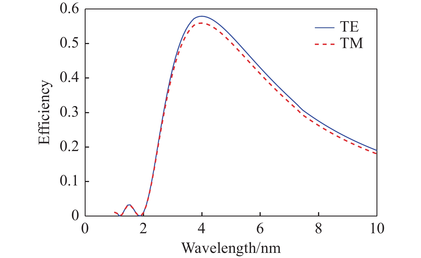
常规成像光谱仪一般变倍比较低,不利于大视场长狭缝多通道光学系统的扩展应用;空间遥感中紫外波段的辐射能量较低,需要成像光谱仪具有更小的F数。针对高光谱分辨率成像光谱仪小F数的探测需求,本文设计了一种具有高变倍的高光谱分辨率Offner紫外成像光谱仪。该成像光谱仪的后置分光系统采用了具有轻小型特点的改进型Offner结构。结合成像光谱仪对变倍比和小F数需求的基础上,通过理论推导得到Offner初始结构参数。在像面前插入一块弯月透镜,增加系统的优化自由度,进而提升系统的成像质量。最终得到的成像光谱仪工作在270~300 nm波段时,具有40 mm的长狭缝,光谱分辨率优于0.6 nm,光谱采样0.15 nm,系统变倍比小于0.22,F数小于2,在截止频率为 14 lp/mm 时,系统调制传递函数(MTF)均优于0.9,系统各波段各视场均方根半径(RMS)均小于12 μm。本文的研究对紫外波段高光谱探测成像光谱仪实现小F数、高变倍设计提供了一种设计方案。

钙钛矿材料具有优异的光学性能和较高的载流子迁移率,成为空间太阳能电池领域极具竞争力的材料。然而空间粒子辐照容易改变材料结构和光学性能,导致其性能下降。为了探究电子辐照对CsPbBr3材料结构与光学特性的影响规律,本文开展了CsPbBr3材料电子辐照实验,利用高分辨透射电子显微镜方法表征CsPbBr3纳米晶微观形貌,并通过X射线衍射分析和X射线光电子能谱分析进一步探究晶体结构的变化趋势。研究发现电子辐照后CsPbBr3纳米晶形貌变得粗糙,尺寸明显减小,并且纳米晶在高剂量电子辐照下变得紧凑,形成纳米团簇。其次通过稳态紫外-可见吸收光谱图与光致发光谱图表征CsPbBr3材料光学性能,并利用第一性原理计算分析辐照后晶格膨胀带来的带隙变化。研究证明电子辐照后纳米晶颜色加深,影响钙钛矿透光率,进而增强了样品对光的吸收性能,同时电子辐照能够分解CsPbBr3纳米晶,特别是高剂量辐照后其光致发光性能显著降低53.7%~78.6%。研究结果为钙钛矿纳米晶空间辐射损伤机理及应用研究提供数据支撑。

设计了一种用于甲烷和氢气同时检测的基于表面等离子体共振(SPR)的新型光子准晶体光纤(PQF)传感器。在该传感器中,在银膜上分别沉积Pd-WO3和掺杂聚硅氧烷的笼型分子E薄膜作为氢气和甲烷的敏感材料。采用全矢量有限元方法对PQF-SPR传感器进行了数值分析,证明了该传感器具有良好的传感性能。在0% ~ 3.5%的浓度范围内,氢气的最大检测灵敏度和平均灵敏度分别为0.8 nm/%和0.65 nm/%,甲烷的最大灵敏度和平均灵敏度分别为10 nm/%和8.81 nm/%。该传感器具有同时检测多种气体的能力,在设备小型化和远程监测方面具有很大的潜力。

光程吸收光谱技术是吸收光谱技术发展中的一个重要分支,近年来基于不同光源技术、吸收腔技术、探测方式的光程吸收光谱技术大量涌现。随着对探测灵敏度和吸收光程长度需求的提高,出现了基于增强吸收原理的光程吸收光谱技术,包括:积分腔光谱(ICOS)、腔增强吸收光谱(CEAS)和腔衰荡光谱(CRDS)。增强吸收光谱技术具有高光谱分辨率、高灵敏度、快速响应、便携等优势,但至今缺乏统一的概念和明确的分类依据。本文梳理了吸收光谱技术的发展历程,明确了多光程吸收光谱技术的概念。依据吸收腔内是否发生谐振吸收,提出了基于谐振原理的吸收光谱技术这一概念,分析总结了谐振吸收光谱技术的研究现状,并对这些技术在各领域的应用进行概述。最后,对谐振吸收光谱技术中关键技术的未来发展进行了展望。

光纤光镊具有结构简单、操作灵活、尺寸小的特点,在生化分析、生命科学等领域有广泛应用。特殊纤芯结构的光纤探针在近场倏逝波光阱力、纤芯光束耦合传输、微流控技术交叉协同应用等方面具有天然优势,能实现细胞、亚细胞级微粒收集、输运等功能,可以显著提升微粒的三维捕获能力以及动态操纵水平。本文综述了不同纤芯结构光纤光镊的结构特点与应用技术研究进展,对特种芯光纤光镊系统中探针制备、金宝搏188软件怎么用 光源、耦合方式等关键技术进行了梳理和对比,总结与展望了不同结构特种芯光纤在光纤光镊中的作用与发展。

氮化镓基Micro-LED具备高亮度、高响应频率、低功耗等优点,是未来显示技术和可见光通信系统的理想选择,但是目前外量子效率(EQE)低下这一问题严重影响其规模化量产及进一步应用。为了突破EQE低下这一瓶颈,通过分析Micro-LED外量子效率的影响因素,得知EQE下降的主要原因包括侧壁缺陷引起的载流子损耗及非辐射复合。总结了侧壁缺陷对载流子输运及复合的影响。综述了目前常用的侧壁处理技术及修复方法,指出现有侧壁处理方法较为笼统、针对性不足且载流子与侧壁缺陷的作用机理并不十分清楚。提出应深入系统地研究侧壁缺陷种类和分布、载流子与侧壁缺陷作用机制及侧壁处理过程中的缺陷修复模式。本文为提高外量子效率、加快Micro-LED商业化量产进程提供设计思路和理论依据。

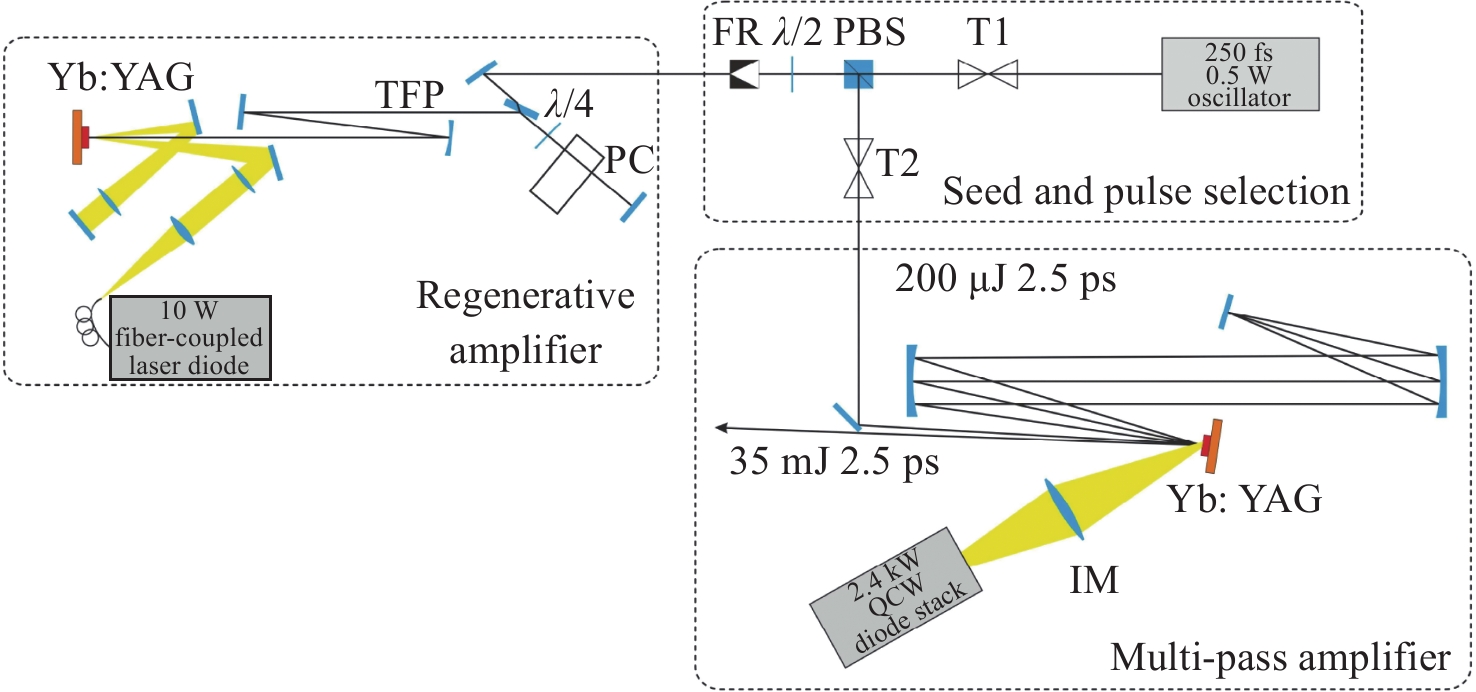
为了提高半导体检测用深紫外金宝搏188软件怎么用 器的检测效率,需要搭建高功率、高重频257 nm深紫外皮秒金宝搏188软件怎么用 器实验平台。本文以光子晶体光纤放大器和腔外四倍频结构为基础,进行了257 nm深紫外金宝搏188软件怎么用 器的实验研究。种子源采用中心波长为1030 nm、脉冲宽度为50 ps的光纤金宝搏188软件怎么用 器,输出功率为20 mW,重复频率为19.8 MHz。通过两级掺镱双包层(65 μm/275 μm)光子晶体光纤棒放大结构,获得了1030 nm高功率基频光。利用二倍频晶体LBO、四倍频晶体BBO,采用腔外倍频方式获得了257 nm深紫外金宝搏188软件怎么用 。种子源通过两级光子晶体光纤放大器输出的1030 nm基频光,输出功率为86 W,经过金宝搏188软件怎么用 聚焦系统后,倍频得到二次谐波515 nm金宝搏188软件怎么用 输出功率为47.5 W,四次谐波257 nm深紫外金宝搏188软件怎么用 输出功率为5.2 W,四次谐波转换效率为6.05%。实验结果表明,该结构可获得高功率257 nm深紫外金宝搏188软件怎么用 输出,为提高半导体检测用金宝搏188软件怎么用 器的检测效率提供了新思路。

太阳光经大气散射与水面折射后会形成有一定分布特性的水下偏振光,利用水下偏振光的偏振分布模式可实现水下导航。本文提出了基于波浪水面下偏振光分布模式的气-水模型,可用于计算大气多次散射后波浪折射影响下水下偏振光的偏振分布模式。模拟并对比分析了平静水面、正弦波浪与随机波浪下,不同太阳高度角的水下偏振光的偏振度和偏振角的分布图像,并通过水下实验进行了验证。水下偏振光模式模拟结果与实测结果的对比表明,利用该模型可以准确表征典型波浪水面下的偏振光分布模式特性,为提高水下偏振导航在水面波动条件下的环境适应性提供理论模型基础。

为了提高金宝搏188软件怎么用 光尾流制导距离和探测信噪比,研究不同距离、不同气泡尺度、不同气泡数密度和不同气泡层厚度的气泡目标的后向散射特性具有重要的理论和应用价值。采用蒙特卡洛仿真和室内实验研究了前述舰船尾流气泡目标的金宝搏188软件怎么用 后向散射特性。结果表明:近距离的气泡要比远距离的气泡更容易被检测到;在气泡数密度为102~108 m−3,气泡层厚度大于0.05 m时,大尺度和小尺度气泡始终存在回波信号,气泡层厚度小于0.05 m时无回波信号,此时,气泡层厚度特性对气泡后向散射的影响最大;在气泡数密度为109 m−3,气泡层厚度为0.05 m以下时,大尺度气泡回波信号脉冲宽度会展宽。在这种情况下,气泡数密度和尺度特性对气泡后向散射的影响最大。搭建了水下典型气泡尺度下的金宝搏188软件怎么用 后向散射测量系统,验证了不同舰船尾流气泡目标特性对金宝搏188软件怎么用 后向探测系统的影响。本文研究成果可为舰船尾流金宝搏188软件怎么用 探测工程提供支撑。

当前光子神经网络的研究主要集中在单一模态网络的性能提升上,而缺少对多模态信息处理的研究。与单一模态网络相比,多模态学习可以利用不同模态信息之间的互补性,因此,多模态学习可以使得模型学习到的表示更加完备。本文提出了将光子神经网络和多模态融合技术相结合的方法。首先,利用光子卷积神经网络和光子人工神经网络相结合构建异构光子神经网络,并通过异构光子神经网络处理多模态数据。其次,在融合阶段通过引入注意力机制提升融合效果,最终提高任务分类的准确率。在多模态手写数字数据集分类任务上,使用拼接方法融合的异构光子神经网络的分类准确率为95.75%;引入注意力机制融合的异构光子神经网络的分类准确率为98.31%,并且优于当前众多先进单一模态的光子神经网络。结果显示:与电子异构神经网络相比,该模型训练速度提升了1.7倍。与单一模态的光子神经网络模型相比,异构光子神经网络可以使得模型学习到的表示更加完备,从而有效地提高多模态手写数字数据集分类的准确率。

聚焦型太阳模拟器可以获得高倍汇聚的太阳辐射光斑,在太阳能热发电及热化学研究领域具有重要应用。为了获得均匀的太阳辐射光斑,提出了基于非成像光学的自由曲面聚光镜设计方法。详细阐述了设计原理与具体方法。设计了自由曲面聚光镜,并将其与包容角相同的非共轴椭球聚光镜进行对比。通过仿真分析验证了设计方法的正确性。仿真结果表明:使用额定功率为6 kW的氙灯作为光源时,自由曲面聚光镜构成的单灯太阳模拟器可以在直径为60 mm的目标面内提供平均辐照度为274.4 kW/m2的光斑,与非共轴椭球太阳模拟器相比,光斑不均匀度从18.28%下降到5.69%;七灯太阳模拟器可以产生平均辐照度为1.65 MW/m2的光斑,光斑不均匀度从13.19%下降到5.79%。

为了产生半径可自由调控的聚焦环形金宝搏188软件怎么用 且确保离焦后光束强度仍均匀,本文提出一种透射-反射式组合的环形光光学系统设计方法。对于透射式系统,基于等能量分割原理,建立入射光与出射光投射高度的映射函数,优化透镜的各项参数,将入射的高斯光先整形成平顶圆形光,实现光束强度均匀化。反射式系统通过调整焦面环形光直径调控范围、工作距离等参数,结合几何光线追迹原理,计算圆锥反射镜、抛物柱面镜及动镜的各项参数,将平顶圆形光再整形成环形光。实验结果表明:当动镜半顶角为16°时,所设计系统能够实现聚焦环形光半径在15~30 mm范围的自由调控,尺寸误差不超过0.05 mm,离焦后强度均匀度达到84%。该设计方法无需更换系统镜片即可兼顾强度均匀性和尺寸自由度,可操作性好,产生的环形光加工精度和效率更高。

变形光学系统具有双平面对称性,其在两个对称面内的焦距不同。利用变形光学系统能够在使用常规尺寸传感器的情况下获得更宽的视场。本文根据变形光学系统的一阶像差特性,提出了一种设计折反式变形光学系统的方法。使用双锥面(Biconic Surface)面型设计了一个折反式变形光学系统。系统在
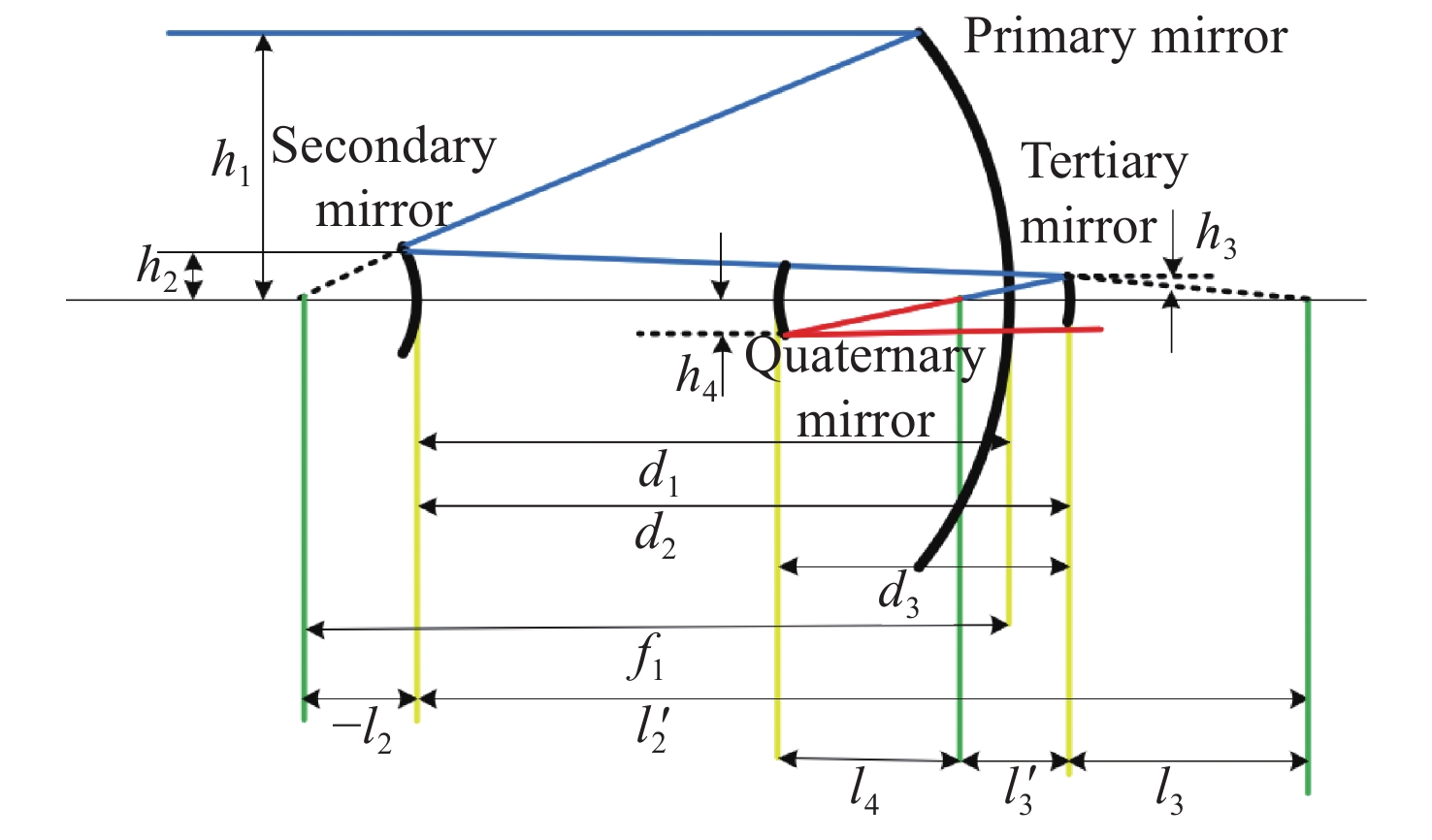
太极计划是中国探测空间引力波的一项重点任务。望远镜作为空间引力波探测中的重要组成部分,它的性能会直接影响引力波探测的精度。现有的典型空间引力波望远镜结构中次镜灵敏度高,难以满足更大口径的空间引力波望远镜对制造装调公差的要求,特别是在轨稳定性公差要求。为解决以上问题,首先,提出了一种中间像面设置于三四镜之间的新型空间引力波望远镜光学系统结构,以降低次镜灵敏度;结合高斯光学理论方法,从理论上分析并计算新型望远镜结构的初始参数。其次,通过优化设计,获得入瞳直径为400 mm,放大倍率为80倍,科学视场为±8 μrad,波前误差RMS值优于0.0063λ的望远镜光学系统。最后,建立了望远镜系统的灵敏度评价公差分配表,对比分析了现有望远镜结构与新型望远镜结构的公差情况。结果显示:相较于现有望远镜结构,新型望远镜结构的灵敏度降低了30.4%,具有低灵敏度优势,为空间引力波望远镜的设计提供了一种优选方案。

太极计划是中国科学院提出的空间引力波探测任务,其利用金宝搏188软件怎么用 差分干涉的方法探测卫星间由引力波引起的pm级位移波动。为消除卫星间因时钟不同步而产生的测量误差,拟采用边带倍频时钟噪声传递方法进行星间时钟噪声测量与消除。本文讨论太极计划星间时钟噪声传递的需求、原理、方法,并设计实验进行原理验证。通过搭建电子学实验测试两个系统时钟噪声的极限值,确定实验相关参数,进一步通过光学实验验证边带倍频传递方案的原理。实验结果表明,本文提出的时钟噪声消除方案及相关参数合理可行,满足太极计划的应用需求。在0.05 Hz~1 Hz频段,星间时钟噪声的抑制效果优于2π×10−5 rad/Hz1/2,满足太极探路者的噪声需求。本文研究为未来太极计划的时钟噪声传递方案与参数设计奠定实验和理论基础。

为了满足惯性传感器地面弱力测量系统的超高温度稳定性要求,对整个系统进行了热设计。首先,介绍了惯性传感器地面弱力测量系统的结构、敏感结构传热路径和内部热源。其次,根据系统热控指标要求,提出了采用三级热控结构和比例积分微分(PID)控制算法相结合的高精度热控方式,减少温度噪声对惯性传感器探测灵敏度的影响。然后,采用UG/NX软件建立有限元模型,并进行了不同工况条件下的热分析计算,得到了惯性传感器地面弱力测量系统在时域上达到平衡后的温度变化值为(1.2~1.6) ×10−5 K。最后,将惯性传感器地面弱力测量系统在时域上的温度分布在频域上进行描述,得到惯性传感器敏感结构的温度稳定性结果。分析结果表明,在当前热控措施下,惯性传感器敏感结构的温度稳定性均优于10−4 K/Hz1/2,满足热控指标需求,热设计方案合理可行。

冷反射现象是指在红外热成像系统中制冷探测器通过前面光学表面的反射而探测到的自身的像,冷反射的控制是红外成像系统的重要任务。本文设计了一款采用Cassegrain(卡塞格林)反射结构的制冷型中波红外成像系统,分析了该系统的冷反射现象,得到了冷反射现象严重的表面。接着,通过Zemax软件降低这些严重面的冷发射,在控制冷反射的同时兼顾系统传递函数MTF的优化。通过NARCISSUS宏命令(冷反射分析宏命令)、Tracepro建模软件和实际成像图将优化后的中波红外成像系统与冷反射抑制前的系统进行比对。结果显示:探测器像面冷反射引入的等效温差( NITD)由1.0484 K下降到了0.1576 K,同时系统在调焦过程中冷反射斑的能量和尺寸无明显变化,优化后的光学结构有效地控制了系统的冷反射。

构建空间目标辐射特性对于发展空间态势感知技术具有重要意义。本文针对空间目标红外辐射特性,基于有限元方法,采用非结构四面体网格研制了仿真程序,通过矢量坐标变换,计算得到了目标各表面受到的轨道外热流,并结合表面材料和双向反射分布函数(BRDF)对目标各表面温度和红外辐射特性进行了仿真,并与文献结果进行了对比。进而考虑大气衰减和背景辐射的影响,对地基探测条件下升轨和降轨弧段的目标光谱辐射强度进行了分析。结果显示:对于三轴稳定太阳同步轨道沿飞行方向固定式帆板卫星,各表面在阳照区和地影区内温度变化范围较小;使用8~14 μm长波波段对目标进行观测的效果比3~5 μm中波波段好;辐射强度最大值在770 W/sr左右;地基红外光谱探测受大气影响较大,需要对探测波段进行优选。

为了提高传统星敏感器的姿态测量精度,可将干涉测角技术与传统星敏感器相结合,即在传统星敏感器质心定位技术的基础上,利用星像点的光强信息进一步进行细分,从而突破了质心定位的精度限制,形成具有大视场高精度的干涉星敏感器。本文对制约干涉星敏感器测角精度的因素进行深入研究,重点研究干涉条纹的分割误差对测角精度的影响机理。通过研究分析,得出以下结论:光锲阵列不等分误差不是影响干涉星敏感器测角精度的主要因素;莫尔条纹周期与光楔阵列整体通光尺寸不匹配误差小于1%时,可保证单因素测角误差小于0.01";对于莫尔条纹取向与光楔阵列排布方向不正交误差,条纹旋转角度应当小于0.1°,可保证单因素测角误差小于0.01"。所以,应在实际加工与装调过程中抑制上述两个主要误差,从而使干涉星敏感器的实际测角精度接近高精度理论值。

单色仪广泛应用于光谱定标、物质分析等方面,因此,对于高光谱分辨率单色仪系统的研究具有重要意义。本文基于矢量光栅方程推导考察了入射狭缝高度对光谱仪器谱线弯曲的影响程度,给出了谱线弯曲同波长、狭缝高度的解析表达式,进而提出了一种基于狭缝高度抑制谱线弯曲的单色仪光谱分辨率优化方案。结合高灵敏度、超快时间响应探测器的性能指标要求,设计了一款光谱分辨率为0.1 nm,波段范围为185 nm~900 nm的三光栅单色仪光学系统,并搭建样机验证狭缝高度对谱线弯曲的影响,进一步探究了狭缝高度对光谱分辨率的影响规律。实验结果表明:在狭缝宽度一定时,对狭缝高度进行优化,可将光谱分辨率从0.32 nm提高至0.1 nm。

为了满足精准高效快速部署航天遥感器对轻小型空间相机的迫切需求,对满足轻小型相机成像的光学系统形式及成像体制进行了详细对比分析,确定了RC+补偿组的光学系统形式,采用小F数+微小像元的成像体制。对比美国鸽子相机的详细参数,设计了500 km轨道高度上可实现3.48 m分辨率的轻小型全铝高分相机。详细介绍了相机的总体结构、光学系统、光机结构、成像电子学及热控设计结果,得到F5.6的RC+补偿组光学设计结果。采用RSA-6061微晶铝合金做为相机反射镜的结构材料,配合一体化硬铝合金高刚性结构。静力学(重力变形和温度变形)仿真分析结果满足光学设计公差要求。动力学仿真分析结果表明:一阶模态为302.92 Hz,具有足够高的动态刚度和安全裕度。成像电子学采用3.2 μm大面阵9 K×7 K探测器低噪声小型化设计。相机热控由卫星平台保证20 °C±4 °C的温度水平。集成测试结果表明:(1)相机中心视场波像差RMS为

为了满足小型化自适应光学系统校正波前畸变的需求,基于系统理论分析设计了一种使用微型音圈驱动器的变形镜。使用电磁理论和有限元方法优化了微型音圈驱动器的结构参数。从热变形、共振频率、耦合系数等多个参数的角度对变形镜进行了优化。最后根据影响函数完成了波前拟合和残差计算。优化后的69单元紧凑型音圈变形镜具有大相位调制量、良好的热稳定性,第一共振频率为2220 Hz。对于PV值为1 µm的前35项泽尼克模式,紧凑型音圈变形镜的拟合残差均小于30 nm。对于复杂随机像差,紧凑型VCDM能够将波前RMS降至原来的10%以下。结果表明,与传统的音圈变形镜相比,紧凑型音圈变形镜具有更高的波前拟合精度。高性能、低成本的紧凑型音圈变形镜在视网膜成像和机载成像系统中具有良好的应用前景。

基于大增益带宽和高热导率晶体的偏振复用金宝搏188软件怎么用 技术可以提高双频金宝搏188软件怎么用 器和双光梳金宝搏188软件怎么用 器在输出光谱范围和功率方面的性能。本文提出一种基于Yb:CALGO晶体的偏振复用金宝搏188软件怎么用 器。将两片与光轴成45°角切割的双折射晶体放置在增益晶体的前后两侧形成三明治结构,利用双折射晶体的偏振特性使腔内金宝搏188软件怎么用 形成只在三明治结构部分具备空间分离其余部分共线的偏振方向互相垂直的两种模式。同时,这种三明治结构既能使单束泵浦光能够自动分离为两束空间分离匹配的泵浦光,也可以使腔内增益晶体放置在腔内模式腰斑位置处,与泵浦光达到更好的模式匹配,提高光泵浦效率。最终测得的金宝搏188软件怎么用 输出功率达到瓦量级并且斜率效率超过30%。在腔内加入标准具后,实现了频差为太赫兹量级的稳定双频金宝搏188软件怎么用 运转。

速度同步性能和抗干扰性是影响双永磁同步电机(dual-PMSM)同步运行动态响应和稳态精度的重要因素。通过引入交叉耦合控制作为模型,提出了一种基于改进双功率趋近律的积分滑模速度跟踪控制器,以减小两台电机之间的速度误差。设计了负载转矩观测器,将观测值引入滑模控制(SMC)趋近律,以提高系统的抗干扰性能。同时,采用模糊比例积分微分(FPID)控制设计了同步控制器,以提高双永磁同步电机的同步性。验证结果表明,当目标转速为800 r/min时,与传统的PI算法相比,所提出的控制方法可以在空载启动时将两台电机的速度同步误差从25 r/min降低到12 r/min,在负载突然转矩下将速度同步误差由7 r/min降低至2.2 r/min,从而提高了同步性和抗干扰性。

为了探究鼎形微环谐振器的耦合区数量对输出的影响,建立了鼎形微环谐振器的物理模型。利用传输矩阵法对鼎形微环谐振器的物理模型进行研究。分析了不同耦合区数量对鼎形微环谐振器输出的影响。实验结果表明,随着耦合区数量的增加,在1.54~1.56 μm工作波长范围内谐振峰的数量增加,半高全宽FWHM越小,品质因子Q则越大,器件的储能性能越好,并且还能实现对特定波长的滤波作用。耦合区数量对鼎形微环谐振器性能有着很大影响,在设计时根据实际需要选择耦合区数量。

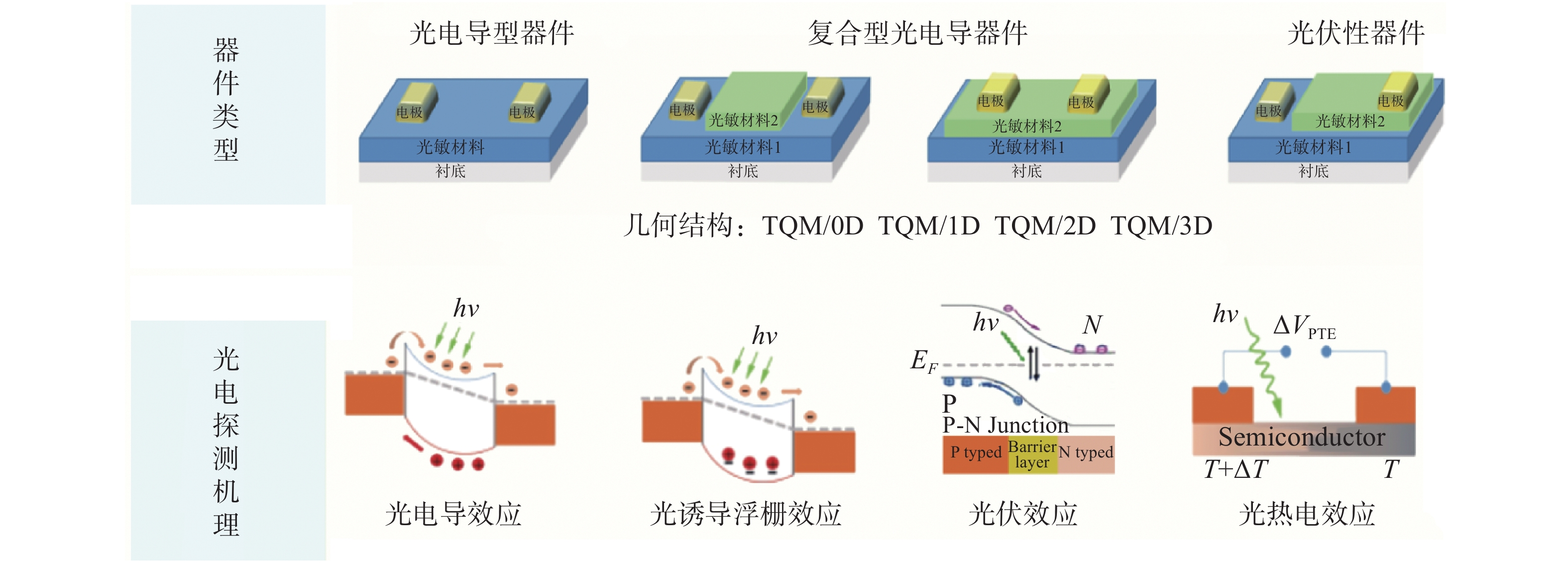
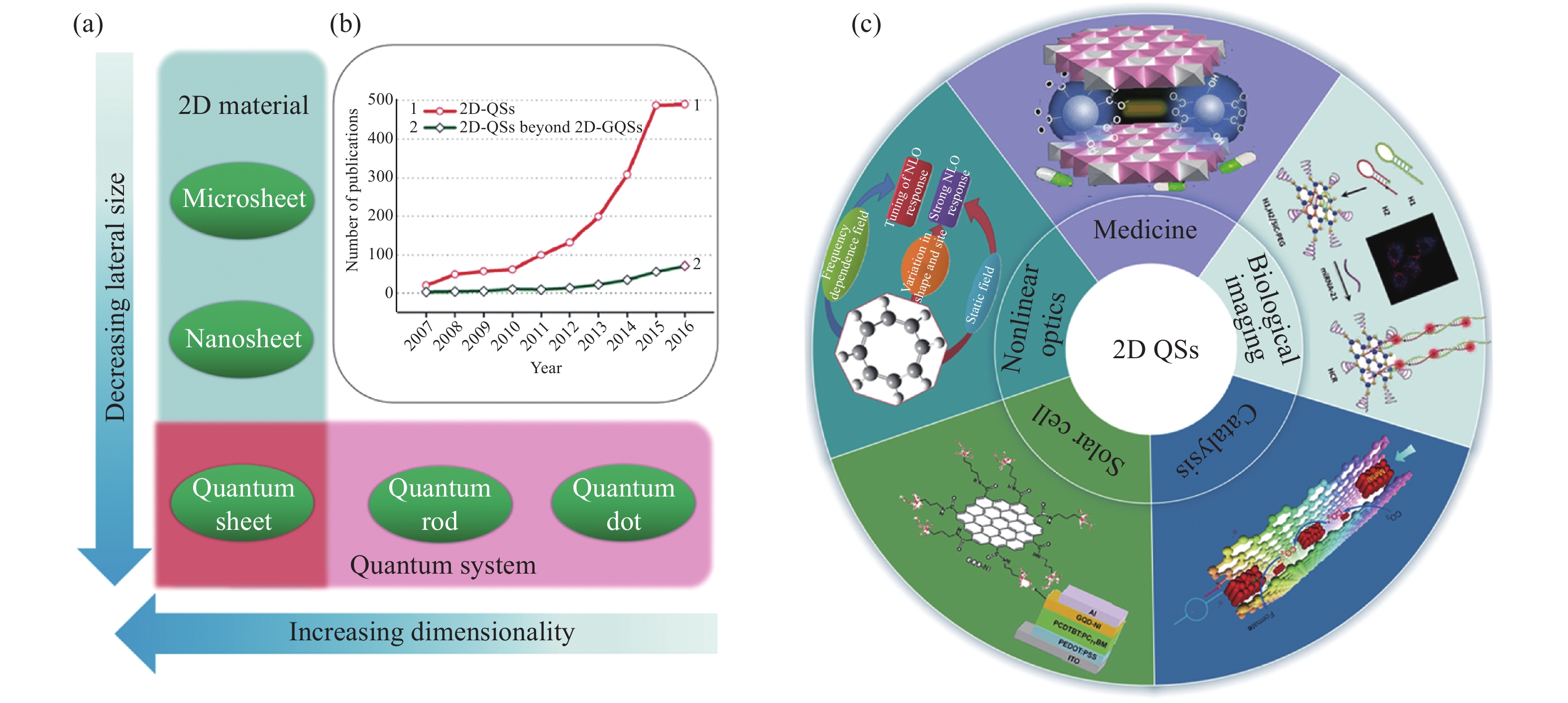
轨道角动量(OAM)是高容量光通信和超分辨成像技术的重要参数。利用惠更斯-菲涅尔原理和相干合成理论,提出了杂化偏振涡旋合成光束阵列。详细研究了涡旋、偏振、附加拓扑电荷及子光束数对输入和输出平面光束的OAM谱的影响。结果表明:子光束的数量和杂化偏振共同影响了OAM模式的最大权重,子光束数量增加会显著提升OAM谱的最大权重,但杂化偏振却不能显著提升OAM谱的最大权重。OAM谱的最大模式位置总是等于光束中心光涡旋的总拓扑数,与子光束数无关。OAM谱所有非零权重模式的位置由涡旋、偏振、附加拓扑电荷和子光束数目共同决定。本文结果对光通信与偏振成像技术有着潜在的应用价值。

腔面光学灾变损伤是导致高功率量子阱半导体金宝搏188软件怎么用 器阈值输出功率受限制的关键因素。通过量子阱混杂技术调整半导体金宝搏188软件怎么用 器腔面局部区域处有源区材料的带隙宽度,形成对输出光透明的非吸收窗口,可提高金宝搏188软件怎么用 器输出功率。本文基于InGaAs/AlGaAs高功率量子阱半导体金宝搏188软件怎么用 器初级外延片,以外延Si单晶层作为扩散源,结合快速热退火方法开展了杂质诱导量子阱混杂研究。探索了介质层生长温度、介质层厚度、热处理温度、热处理时间等条件对混杂效果的影响。结果表明,50 nm的650 °C低温外延Si介质层并结合875 °C/90 s快速热退火处理可在保证光致发光谱的同时获得约57 nm的波长蓝移量。能谱测试发现,Si杂质扩散到初级外延片上的波导层是导致量子阱混杂效果显著的关键。
光程吸收光谱技术是吸收光谱技术发展中的一个重要分支,近年来基于不同光源技术、吸收腔技术、探测方式的光程吸收光谱技术大量涌现。随着对探测灵敏度和吸收光程长度需求的提高,出现了基于增强吸收原理的光程吸收光谱技术,包括:积分腔光谱(ICOS)、腔增强吸收光谱(CEAS)和腔衰荡光谱(CRDS)。增强吸收光谱技术具有高光谱分辨率、高灵敏度、快速响应、便携等优势,但至今缺乏统一的概念和明确的分类依据。本文梳理了吸收光谱技术的发展历程,明确了多光程吸收光谱技术的概念。依据吸收腔内是否发生谐振吸收,提出了基于谐振原理的吸收光谱技术这一概念,分析总结了谐振吸收光谱技术的研究现状,并对这些技术在各领域的应用进行概述。最后,对谐振吸收光谱技术中关键技术的未来发展进行了展望。


光纤光镊具有结构简单、操作灵活、尺寸小的特点,在生化分析、生命科学等领域有广泛应用。特殊纤芯结构的光纤探针在近场倏逝波光阱力、纤芯光束耦合传输、微流控技术交叉协同应用等方面具有天然优势,能实现细胞、亚细胞级微粒收集、输运等功能,可以显著提升微粒的三维捕获能力以及动态操纵水平。本文综述了不同纤芯结构光纤光镊的结构特点与应用技术研究进展,对特种芯光纤光镊系统中探针制备、金宝搏188软件怎么用 光源、耦合方式等关键技术进行了梳理和对比,总结与展望了不同结构特种芯光纤在光纤光镊中的作用与发展。


氮化镓基Micro-LED具备高亮度、高响应频率、低功耗等优点,是未来显示技术和可见光通信系统的理想选择,但是目前外量子效率(EQE)低下这一问题严重影响其规模化量产及进一步应用。为了突破EQE低下这一瓶颈,通过分析Micro-LED外量子效率的影响因素,得知EQE下降的主要原因包括侧壁缺陷引起的载流子损耗及非辐射复合。总结了侧壁缺陷对载流子输运及复合的影响。综述了目前常用的侧壁处理技术及修复方法,指出现有侧壁处理方法较为笼统、针对性不足且载流子与侧壁缺陷的作用机理并不十分清楚。提出应深入系统地研究侧壁缺陷种类和分布、载流子与侧壁缺陷作用机制及侧壁处理过程中的缺陷修复模式。本文为提高外量子效率、加快Micro-LED商业化量产进程提供设计思路和理论依据。


作为一种新型光电探测技术,偏振成像可同时获取场景的空间分布和偏振特征,针对特定应用场景具有优异的材质区分及轮廓辨识能力,广泛应用于目标探测、生命科学、环境监测、三维成像等领域。偏振分光或滤光器件是偏振成像系统的核心元件,然而该类传统器件受限于体积庞大、性能不佳、易受干扰等问题,难以满足高集成、高性能、高可靠性偏振成像系统的要求。超构表面是一种结构单元以亚波长间隔准周期排列而成的二维平面器件,可在不同偏振方向对光场的振幅、相位进行精细操纵。基于超构表面的偏振器件具有体积小、重量轻、维度高等特点,为集成化偏振成像系统提供了新的解决方案。本文针对偏振成像,综述相关超构表面的功能原理、发展脉络和未来趋势,讨论并展望其在成像应用和系统集成方面所面临的挑战与机遇。


为了明晰碟片多通放大器的腔体设计方法,本文对不同类型的碟片多通放大器做归纳与总结,共归纳出4


微型头戴式单光子荧光显微成像技术是近些年出现的用于神经科学研究的一种突破性方法,可以对自由移动活体动物的神经活动进行实时成像,提供了一种前所未有的方式来访问神经信号,增强了对大脑如何工作的理解。在脑科学研究需求的推动下,目前已经出现了许多种类型的微型头戴式单光子荧光显微镜,如高分辨率成像、无线记录、三维成像、双区域成像和双色成像等。为了更加全面地了解和认识这种新兴的光学神经成像技术,本文按成像视场进行分类,对目前报道的不同类型微型头戴式单光子荧光显微镜所具有的特点进行了介绍,重点讨论了其所采用的光学系统方案和光学性能参数,分析对比了不同方案的优缺点,以及未来的改进方向,以便为脑科学研究人员的实际应用提供参考。


非视域(Non-Line-of-Sight, NLoS)成像是近年来发展起来的一项新兴技术,其通过分析成像场景中的中介面信息来重建隐藏场景,实现了“拐弯成像”的效果,在多个领域有巨大的应用价值。本文主要针对NLoS成像重建算法进行综述性研究。考虑到目前NLoS成像分类存在交叉和非独立现象,本文基于物理成像模式和算法模型的不同特点,对其进行了独立的重新分类。根据提出的分类标准分别对传统和基于深度学习的NLoS成像重建算法进行了归纳总结,对代表性算法的发展现状进行了概述,推导了典型方法的实现原理,并对比了传统重建方法和基于深度学习的NLoS成像重建算法的重建应用结果。总结了NLoS成像目前存在的挑战和未来的发展方向。该研究对不同类型的NLoS成像进行了较为全面的梳理,对NLoS成像重建算法在内的一系列研究的进一步发展有着一定的支撑和推动作用。


光致热弹光谱是一种基于石英音叉热弹效应的新型气体检测技术,具有成本低、体积小、灵敏度高及光谱响应范围宽等优点,是目前一种重要的痕量气体检测方法。本文首先分析了基于光致热弹光谱的气体浓度测量原理,其次,从提高检测系统灵敏度的各种技术方法角度出发,介绍了近年来开发的提高石英音叉热弹光谱系统检测灵敏度的技术方法,从信号幅值、信噪比、最小检出限和归一化噪声等效吸收系数等方面,对系统的性能改进提升效果进行评估。最后,简要评述了光致热弹光谱在现场气体检测中的应用研究进展,对进一步提高检测系统灵敏度的方法进行了总结与展望。


温度、湿度、压强是3个重要的大气参数。快速、准确地了解大气的温度、湿度和压强信息及其变化趋势,对天气、气候、人工影响天气等研究有重要意义。拉曼金宝搏188软件怎么用 雷达通过分离拉曼散射信号反演得到各种大气环境相关参数,可实现对大气参数廓线信息的高精度探测,在大气温湿压探测中独具优势与潜力。本文介绍了拉曼金宝搏188软件怎么用 雷达对大气温度、湿度和压强的探测原理与反演方法,着重介绍了拉曼金宝搏188软件怎么用 雷达中滤光片、标准具、光栅等常用分光器件的优缺点及其进展,以及拉曼金宝搏188软件怎么用 雷达中涉及到的探测技术。最后例举了利用拉曼金宝搏188软件怎么用 雷达对气象参数测量的典型应用。


随着光学成像技术的不断发展和遥感应用需求的日益增长,跨尺度高分辨率光学技术在遥感领域得到广泛应用。为了获得更多的目标细节信息,国内外研究学者在不同技术方向开展了相关研究。本文对遥感成像技术进行了总结分类,介绍了具有代表性的航天高分辨率对地光学遥感载荷技术,重点关注单体结构主镜、可展开分块拼接主镜、光学干涉主镜、光栅衍射主镜、虚拟合成孔径、光子型综合孔径成像、计算超分辨成像、编队合成孔径等成像模式,为高分辨率对地光学遥感载荷发展提供新的发展思路。


随着金宝搏188软件怎么用 技术的飞速发展,金宝搏188软件怎么用 在医疗领域中的应用得到了日益广泛的关注。由于其具有无接触、精度高、损伤小、便携性和操作灵活等优点,金宝搏188软件怎么用 医疗极大地丰富了临床医疗的技术手段,在部分疾病的治疗中逐渐取代了传统方法,提升了医疗行业整体的技术水平。当前,金宝搏188软件怎么用 医疗的市场占有率不断增加,发展前景十分广阔。本文介绍了金宝搏188软件怎么用 医疗技术和医用金宝搏188软件怎么用 系统的要求,重点对金宝搏188软件怎么用 医疗在各临床科室中的应用研究现状进行了全面阐述,最后针对我国金宝搏188软件怎么用 医疗领域存在的问题给出了建议。


周期光学系统,如光子晶体和光学超材料,可以在亚波长尺度形成高密度的电磁场能量局域,并获得极小的模式体积,在光操控领域具有巨大的应用潜力。近年来,研究人员在周期光学系统中发现一种光与物质的强相互作用,其被称为连续域束缚态。它是一类频率位于辐射连续域内但被完全局域的特殊电磁本征态,具有诸多有趣的物理特性和丰富的应用场景。本文系统性综述了周期光学系统中连续域束缚态的分类及其理论体系,并总结了其基本物理特性和最新应用发展。周期光学系统中的连续域束缚态正在为集成光学、信息光学、生物光学、拓扑光学以及非线性光学等领域注入新的发展动力。


二维(2D)半导体材料Bi2O2Se由于具有独特的晶体结构与能带结构、超高的载流子迁移率和优异的稳定性,在紫外-可见-近红外光谱区的高性能电子与光电应用领域有着广阔的前景。本文综述了Bi2O2Se的材料制备与光学表征最新研究进展:首先,介绍了2D Bi2O2Se的制备方法及生长机理,包括化学气相沉积法(CVD)、湿化学工艺、分子束外延法(MBE)和脉冲金宝搏188软件怎么用 沉积法(PLD)等;其次,介绍了其晶体结构和电子能带结构的基本性质;接下来,通过稳态光谱的研究,可以对2D Bi2O2Se随厚度变化的带隙等物理性质进行研究;通过研究其晶体振动模式,可进一步研究2D Bi2O2Se材料的缺陷形态、温度系数与热导率;此外,超快光谱技术也可以帮助研究2D Bi2O2Se材料内部载流子的弛豫过程与输运性能;最后,简述了当前Bi2O2Se研究面临的挑战与应用的前景。


全景内窥成像技术可有效减小体内器官的观察盲区,具有缩短手术时间、降低术中出血风险、改善手术预后、缩短术后恢复时间等多种优点,在微创手术和术前检查中有重要应用价值,是近年来的研究热点。本文从原理和产品应用两个方面对全景内窥成像技术进行了梳理。首先,综述了基于二维和三维成像的各种全景内窥成像技术,阐述了它们各自的实现方式,并分析了其关键指标和性能。其次,对比分析了由全景内窥成像技术衍生出来的胶囊内窥镜、全景结直肠镜等多种不同类型的产品,并展望了全景内窥成像技术的发展趋势和应用前景。


单片集成式主振荡功率放大器(MOPA)具有体积小、功率大、光束质量高等优势,通过集成布拉格光栅,还能够实现窄线宽和动态单模,在倍频、泵浦、光通信和传感等领域具有重要应用价值,是近年来半导体光电子器件的研究热点。本文梳理了单片集成式MOPA的主流结构,包括锥形、脊型、布拉格光栅型和三段式MOPA,以各自的工作原理和性能特征为出发点,介绍其主要的研究方向,并结合它们各自面临的问题介绍最新的发展趋势。针对单片集成式MOPA中普遍存在的高功率下光束质量退化的问题,梳理了近年在外延层结构、腔面光学薄膜和电极设置等方面的优化设计,重点总结了单片集成式MOPA在提高光束质量及高功率、容线宽及高亮度方面的重要进展。围绕不同领域的应用需求,整理了具备高功率、窄线宽、高光束质量和高亮度等性能特征的单片集成式MOPA的研究进展,最后展望了单片集成式MOPA的发展趋势。


稀土掺杂的上转换发光纳米材料在信息安全、生物医学、光纤通信、显示和能源等众多领域有着巨大的应用潜力,受到了相关各领域研究人员的广泛关注。特别是近年来发展起来的具有正交激发发射特性的上转换发光纳米颗粒,其可在不同的激发条件下产生动态变化的光色输出,因而具备一系列新的特性与功能,大大地扩展了应用范围。本文综述稀土离子正交上转换发光的发展历程,系统论述了基于核壳结构的正交激发发射体系的设计原理和构建方法,介绍了其在信息存储、安全防伪、显示、传感、生物成像及治疗等领域的最新研究进展,并探讨了未来相关研究中可能面临的机遇和挑战。


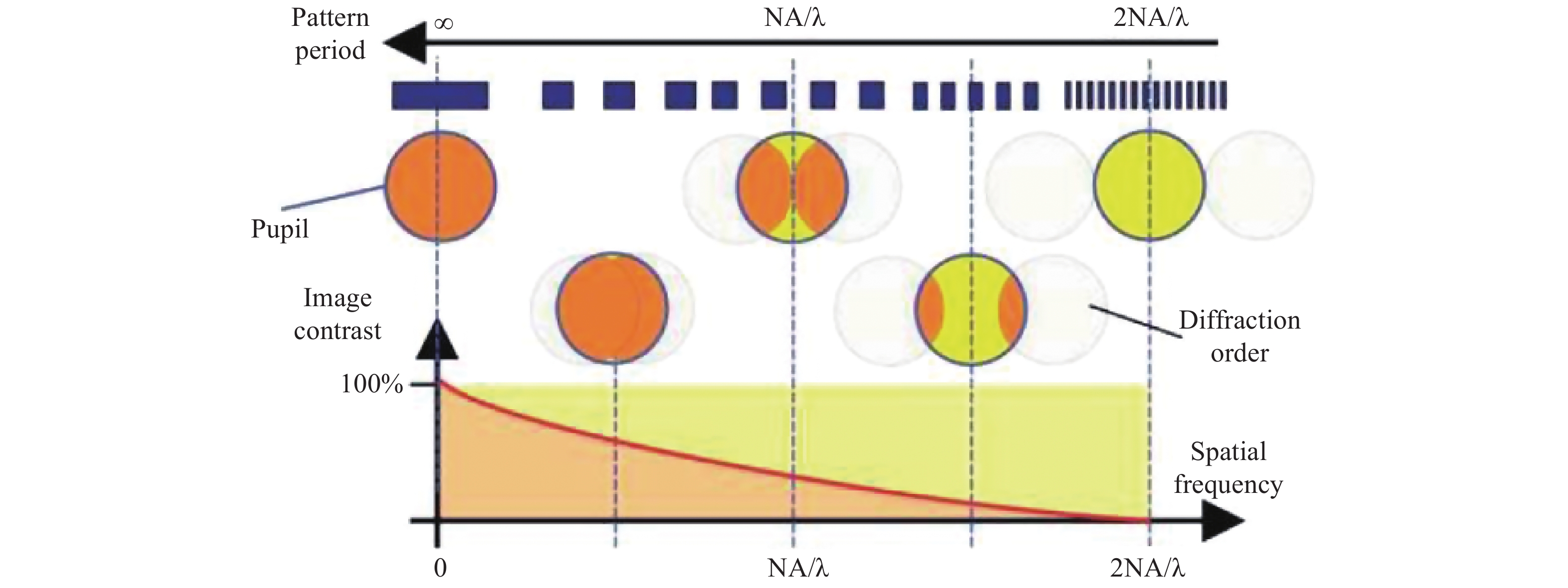
传统光学成像实质上是场景强度信号在空间维度上的直接均匀采样记录与再现的过程。在此过程中,成像的分辨率与信息量不可避免地受到光学衍射极限、探测离散器采样、成像系统空间带宽积等若干物理条件制约。如何突破这些物理限制,获得分辨率更高,视场更宽广的图像信息,是该领域的永恒课题。本文概括性地介绍了分辨率、超分辨率与空间带宽积拓展的相关基础理论,核心机理及其在计算光学成像中的若干实例。通过将这些具体个案置入“计算光学成像”这个更高维度的体系框架去分析与探讨,揭示了它们大多数都可以被理解为一种可称作“空间带宽积调控”策略,即利用成像系统的可用自由度,在成像系统有限空间带宽积的限制下,以最佳方式进行编解码和传递信息的过程,或者形象地说——“戴着脚镣跳舞”。这实质上是一种在物理限制下,在“得”与“失”之间所作出的符合规律的权衡与选择。本文的结论有望为设计和探索面向各类复杂现实成像应用的新型成像机理与方法提供有益启示。


双光子显微镜在厚生物组织中依然可以保持良好的空间分辨率,这一优点使得其诞生不久就被应用于在体脑成像研究。而神经网络在时空多个维度均具有跨尺度的特点,为满足脑科学研究中在体跨尺度脑成像的需求,双光子显微镜近年来有了快速且显著的发展。本文首先介绍了双光子显微镜的工作原理,然后在成像视野、成像通量、成像深度、分辨率、微型化5个方面详细综述了双光子显微镜研究的新进展,并深入分析了跨尺度双光子在体显微成像技术的难点及未来挑战。


光学成像已成为跨尺度表征生物系统信息的主要方法之一,近年来生物样本的快速、无损且全面表征对成像系统的可解析量提出了更高的要求。数字全息通过干涉成像方式,可准确重构光波前的振幅和相位信息,具有快速、无损、三维成像等优势,在数字病理诊断、细胞无标记观察和实时监测等方面得到了广泛的研究和应用。本文首先介绍了实现高通量成像的主要方式,并分析了数字全息的优势及空间带宽变化,展示了基于希尔伯特变换的面向高通量多通道复用数字全息技术的理论框架,并介绍了基于该理论框架设计的拓展视场双通道复用数字全息显微成像系统。该系统在不牺牲空间和时间分辨率的情况下,可实现超越传统离轴全息显微镜8倍的空间带宽积。所介绍的数字全息复用技术可充分利用单幅强度图像的冗余空间带宽,可用于高通量多通道复用数字全息成像。


光学显微成像技术具有实时性、高分辨率和非侵入性等特点,其成像尺度可跨越细胞、组织乃至生命体,极大地拓展了人们对生命本质的认识边界。然而,受限于光学显微成像系统有限的空间带宽积(Space-Bandwidth Product,SBP),常规的光学显微镜难以同时兼具大视场和高分辨率,使得显微成像在大视场生物成像应用中受到较大的限制,例如,对脑神经网络以突触为单位的神经回路成像。近年来,大视场光学显微成像技术得到不断的发展,其SBP的视场相较于传统的光学显微镜有了十倍甚至百倍的提升,在保持高分辨率的基础上拓展了成像视场,从而可以满足生物医学领域重大问题的研究需求。本文介绍了近年来几种典型的大视场光学显微成像技术及其生物医学应用,并对其未来发展做了展望。


- 2023 5期 4期 3期 2期 1期
- 2022 6期 5期 4期 3期 2期 1期
- 2021 6期 5期 4期 3期 2期 1期
- 2020 6期 5期 4期 3期 2期 1期
- 2019 6期 5期 4期 3期 2期 1期
- 2018 6期 5期 4期 3期 2期 1期
- 2017 6期 5期 4期 3期 2期 1期
- 2016 6期 5期 4期 3期 2期 1期
- 2015 6期 5期 4期 3期 2期 1期
- 2014 6期 5期 4期 3期 2期 1期
- 2013 6期 5期 4期 3期 2期 1期
- 2012 6期 5期 4期 3期 2期 1期
- 2011 6期 5期 4期 3期 2期 1期
- 2010 6期 5期 4期 3期 2期 1期
- 2009 6期 5期 4期 3期 2期 1期
- 2008 1期