Design of all-optical logic gate based on two-dimensional photonic crystal
doi: 10.37188/CO.EN-2023-0014
-
摘要:
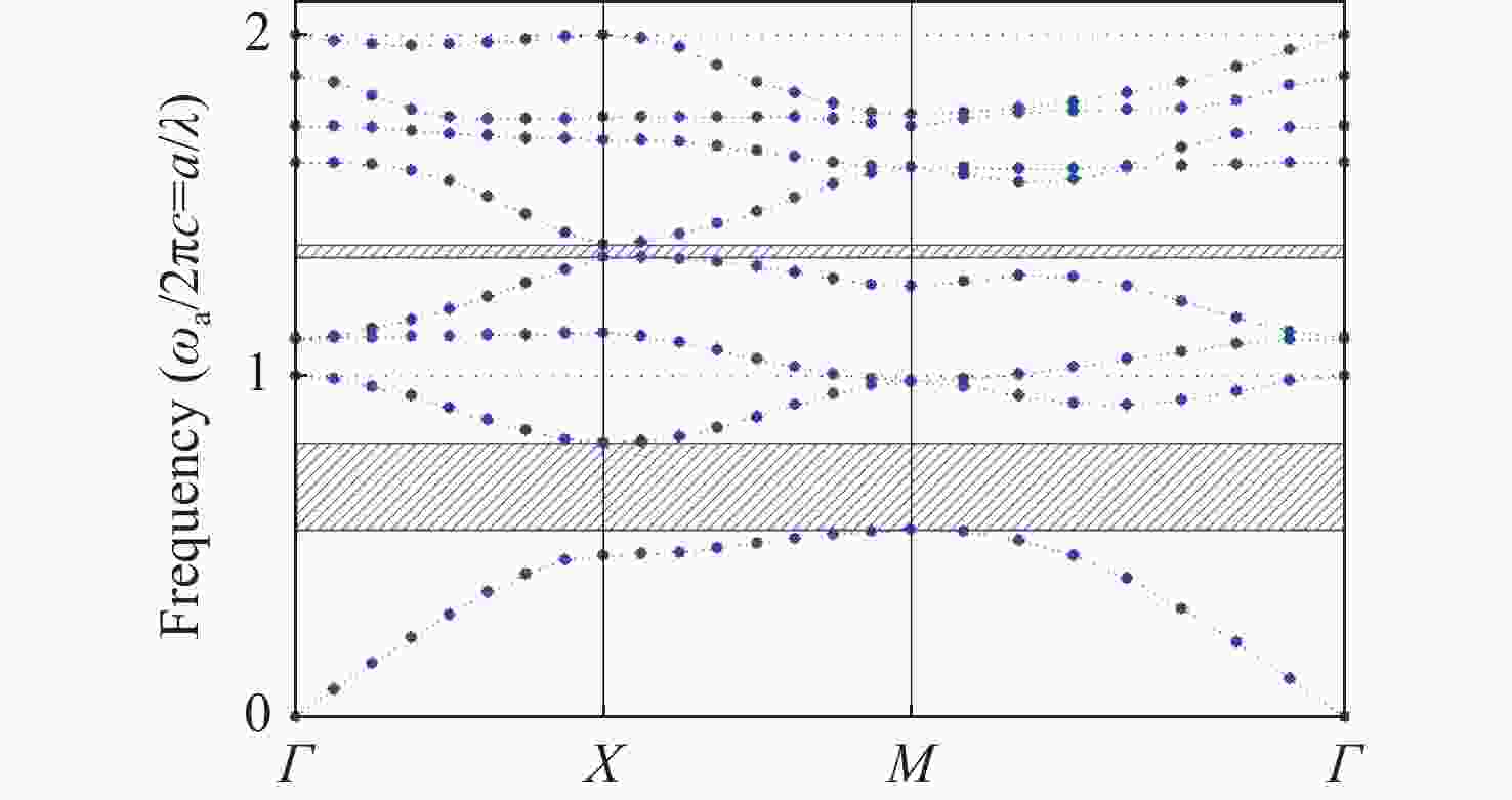
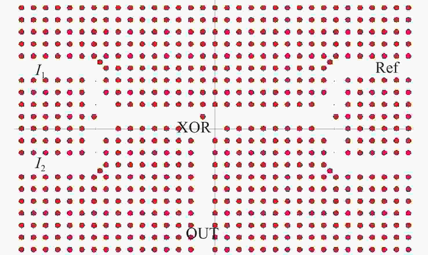
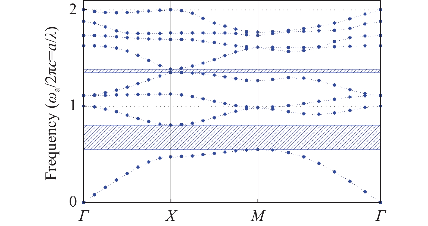
在二维光子晶体中嵌入了线缺陷,利用线性干涉效应和波导耦合,设计了一种基于二维光子晶体的同或门和与非门结构。主要采用平面波展开法对该二维光子晶体的能带结构进行分析,采用时域有限差分法,结合线性干涉效应,在Rsoft平台对所设计的同或门和与非门进行稳定电场图和归一化功率仿真。仿真结果标明:设计的同或门对比度高达29.5 dB,响应时间为0.073 ps,数据传输速率为13.7 Tbit/s;设计的与非门对比度高达24.15 dB,响应时间为0.08 ps,数据传输速率为12.5 Tbit/s。这些结果表明所设计的结构对比度高、响应时间短和数据传输速率快。
Abstract:By embedding a line defect in a two-dimensional photonic crystal and using linear interference effect and waveguide coupling, an XNOR gate and NAND gate structure based on a two-dimensional photonic crystal is designed. The band structure of the two-dimensional photonic crystal is analyzed by using the plane wave expansion method. The time-domain finite-difference method and the linear interference effect are used to simulate the stable electric field diagram and the normalized power of the XNOR gate and NAND gates on the Rsoft platform. The simulation results demonstrate that the designed XNOR gate has a contrast of 29.5 dB, a response time of 0.073 ps, and a data transmission rate of 13.7 Tbit/s. On the other hand, the designed NAND gate has a contrast of up to 24.15 dB, a response time of 0.08 ps, and a data transmission rate of 12.5 Tbit/s. It can be seen that the designed structure has a high contrast, short response time, and fast data transmission rate.
-
Key words:
- photonic crystal /
- logic gate /
- finite difference time domain method /
- interference /
- contrast
-
Figure 6. The stable electric field diagram and normalized power curve when the input logic is '00', '10' and '11', respectively. (a)-(c) are electric field diagrams when input logic is (a) '00', (b) '10', and (c) '11'; (d)-(f) are normalized curves when input logic is (d) '00', (e) '10', and (f) '00'
Table 1. Summarized features of proposed structure and previous works
-
[1] CHEN H M, WEI X Y. The design of high-speed photonic crystal optical switch[J]. Opto-Electronic Engineering, 2013, 40(11): 34-39. (in Chinese). [2] KONG X D. Development status of electronic technology application system[J]. Electronic Technology & Software Engineering, 2017, (1): 115. (in Chinese) [3] GUO Y, ZHU J F, ZHANG H, et al. Research on all-optical switch based on nonlinear effect of photonic crystal[J]. Imaging Science and Photochemistry, 2020, 38(1): 15-21. (in Chinese). doi: 10.7517/issn.1674-0475.190713 [4] SHAIK E H, RANGASWAMY N. Multi-mode interference-based photonic crystal logic gates with simple structure and improved contrast ratio[J]. Photonic Network Communications, 2017, 34(1): 140-148. doi: 10.1007/s11107-016-0683-7 [5] GUPTA P, PALTANI P P, TRIPATHI S. Photonic crystal based all-optical switch using a ring resonator and Kerr effect[J]. Fiber and Integrated Optics, 2022, 41(5-6): 143-153. doi: 10.1080/01468030.2022.2163725 [6] LIANG L X, ZHANG X J, WU X S, et al. Terahertz filter and optical switch based on magnetic-photonic crystals[J]. Acta Optica Sinica, 2018, 38(5): 0513002. (in Chinese). doi: 10.3788/AOS201838.0513002 [7] FU P D, CHEN H M. Design and performance analysis of three-mode division multi/demultiplexer based on two-dimensional photonic crystals[J]. Laser & Optoelectronics Progress, 2017, 54(2): 020602. (in Chinese). [8] THARA R L, PRIYA P A, NAYAK C. Si-SiO2 clustery random photonic crystal based thermo-optic sensor[J]. Silicon, 2022, 14(18): 12919-12929. doi: 10.1007/s12633-022-01984-1 [9] AOBAID R A, HUSSAIN H S. Magneto-optical sensor based on the bandgap effect of a hollow-core photonic crystal fiber injected with Fe3O4[J]. IOP Conference Series:Materials Science and Engineering, 2020, 871(1): 012068. doi: 10.1088/1757-899X/871/1/012068 [10] LIU ZH, WU R, YAN Q B, et al. Design and simulation of two-dimensional photonic crystal all-optical logic gates[J]. Laser & Optoelectronics Progress, 2019, 56(18): 182301. (in Chinese). [11] WU R, ZHAO CH Q, HE ZH X. Design and optimization of all-optical NOR and NOT logic gates[J]. Semiconductor Optoelectronics, 2017, 38(1): 45-48. (in Chinese). [12] 孙晓雯. 基于二维光子晶体自准直效应的全光逻辑门研究[D]. 济南: 山东大学, 2018.SUN X W. Research on all-optical logic gate based on the self collimation effect of 2D photonic crystal[D]. Ji’nan: Shandong University, 2018. (in Chinese). [13] 刘振. 基于二维光子晶体逻辑门的全光加法器研究[D]. 兰州: 兰州交通大学, 2020.LIU ZH. Research on all-optical adder based on two-dimensional photonic crystal logic gates[D]. Lanzhou: Lanzhou Jiaotong University, 2020. (in Chinese). [14] CHHIPA M K, MADHAV B T P, SUTHAR B, et al. Ultra-compact with improved data rate optical encoder based on 2D linear photonic crystal ring resonator[J]. Photonic Network Communications, 2022, 44(1): 30-40. doi: 10.1007/s11107-022-00975-x [15] CAI CH, JIANG Z D, LI P L. Fast all-optical 4×2 encoder with high contrast based on two-dimensional photonic crystal[J]. Laser & Optoelectronics Progress, 2022, 59(1): 0114004. (in Chinese). [16] ZHANG Y, LI M F, CHEN D Y. Design and optimization of half-adder based on two-dimensional photonic crystal[J]. Laser & Optoelectronics Progress, 2022, 59(1): 0123001. (in Chinese). [17] BOUAOUINA M S, LEBBAL M R, BOUCHEMAT T, et al. High contrast ratio for full-designs optical logic gates based on photonic crystal ring resonator[J]. Frequenz, 2020, 74(9-10): 277-285. doi: 10.1515/freq-2020-0011 [18] CABALLERO L P, POVINELLI M L, RAMIREZ J C, et al. Photonic crystal integrated logic gates and circuits[J]. Optics Express, 2022, 30(2): 1976-1993. doi: 10.1364/OE.444714 [19] VADIVU N S, TRABELSI Y, JAYASINGH J R, et al. A novel design of all logic gates in honeycomb photonic crystal and independent of polarization modes (TE/TM) for optical integrated circuit applications[J]. Optics and Lasers in Engineering, 2023, 161: 107345. doi: 10.1016/j.optlaseng.2022.107345 -


 下载:
下载:


