Optical simulation design of surface mounted device beads for wide beam and high uniformity display
doi: 10.37188/CO.EN-2023-0017
-
摘要:
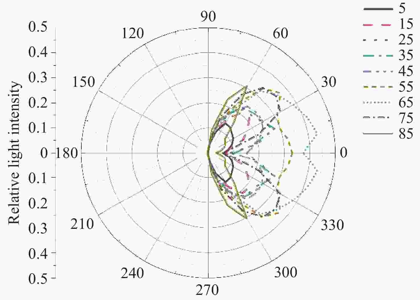
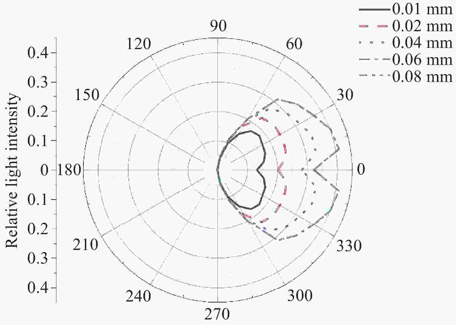
本文通过分析目前显示器用的高均匀宽角度灯珠的光学要求,采用新型非朗伯(non-Lambertian)分布封装Micro-LED芯片,实现了宽光束、高均匀性的微型LED芯片光珠。分析了在不同封装倾角、封装高度、封装材料、封装支架材料、蓝宝石厚度和图案化蓝宝石衬底尺寸下,使用由不同封装材料(铜、钛、铝和银)和材料类型(完全反射和完全吸收)组成的支架模拟固定灯珠的光输出效率和出光角度的变化情况。研究发现通过调整材料、芯片和封装参数,可以得到一个、两个或三个光束,具有贴片灯珠的宽角度、高均匀性的远场光分布特性,满足当前LED和LCD的显示要求。
Abstract:Through analysing the optical requirements of wide beam and high uniformity light beads, which are currently used in displays, and packaging micro Light-Emitting Diode (LED) chips with a novel non-Lambertian distribution, we realized the production of wide beam and high uniformity micro-LED chip light beads. The light output efficiency and beam angle of fixed beads were simulated using brackets made of copper, titanium, aluminium and silver, as well as materials that were completely reflecting and absorbing. The simulations were conducted at various fixture angles, packaging heights, packaging materials, sapphire thicknesses, and patterned sapphire substrate sizes. By adjusting the chip and packaging parameters, we can obtain one, two, or three light beams with Surface Mounted Device (SMD) lamp beads characteristics that provide wide angles, high uniformity, and far-field light distribution. These characteristics can meet the current display requirements for LED and LCD.
-
Key words:
- non-lambertian distribution /
- lambertian distribution /
- displays /
- SMD lamp beads
-
Table 1. Simulated optical parameters of different bracket materials
Material Refractive index Absorption index/(mm−1) Cu 1.15 65889 Al 0.7278 152263 Ag 0.886 113067 Ti 1.71 62667 Perfect absorption - 1 Perfect reflection 1 - Table 2. Simulated optical parameters of different packaging materials
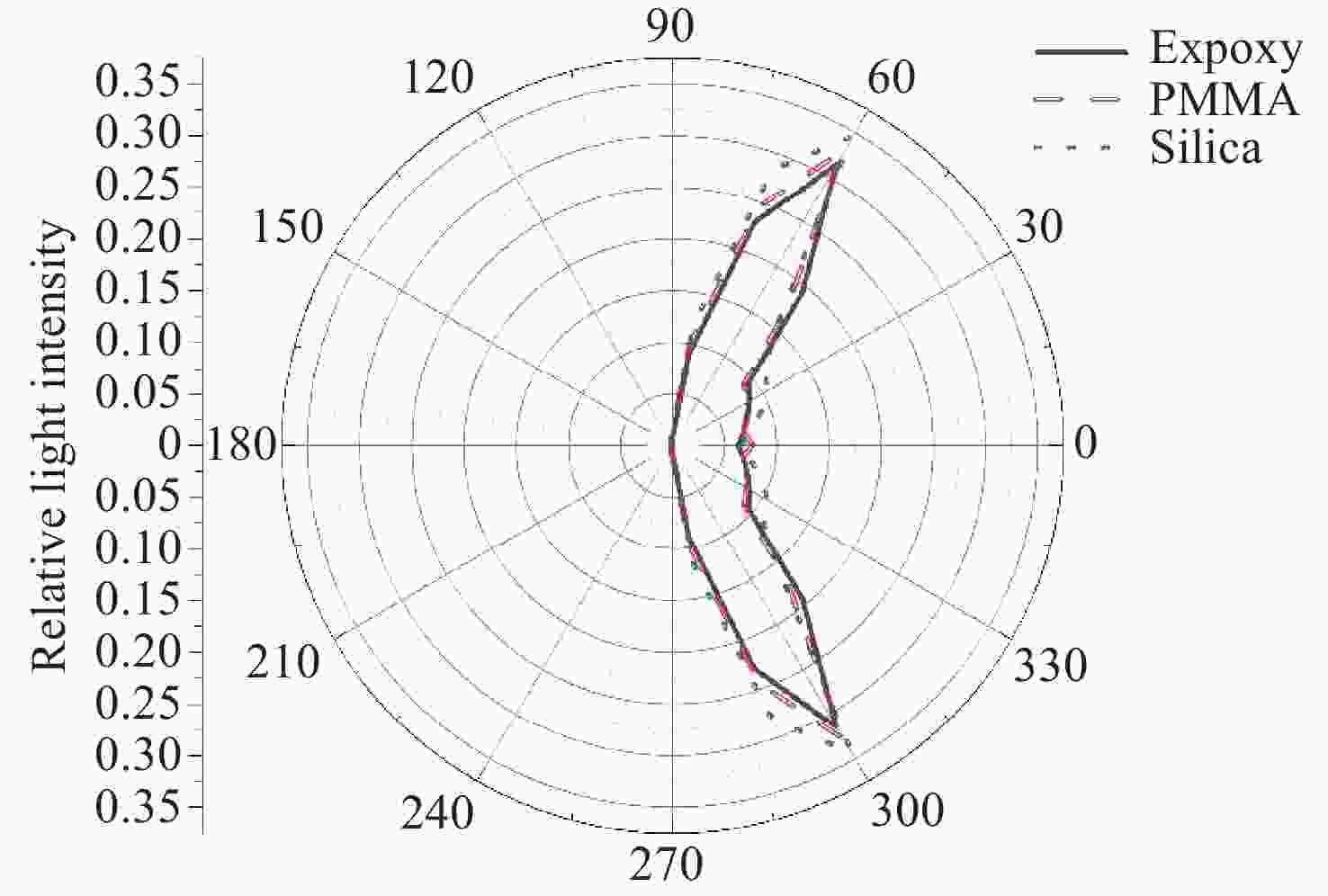
Material Refractive index Absorption index/(mm−1) Epoxy 2.605 0.0078 PMMA 1.499 0 Silica 1.41 0.01 Table 3. Simulated optical parameters of light-emitting diodes with different sizes
Material Thickness Refractive
indexAbsorption index/
(mm−1)Sapphire 30 µm 1.70 0.004 ITO 300 nm 1.50 0 p-GaN 150 nm 2.45 2.300 Active layer (MQW) 100 nm 2.54 25 n-GaN 6.75 µm 2.45 2.3 Table 4. Far-field beam angle and output efficiency of 5050 SMT beads with Al bracket and PMMA packaging materials at different angles
Width of
square/mmLight-beam
angleLight extraction
efficiencyNumber of
light beams5 70 0.288 2 15 50 0.400 2 25 70 0.489 2 35 70 0.505 2 45 160 0.508 1 55 140 0.652 1 65 120 0.654 1 75 50 0.645 2 85 30 0.454 2 Table 5. Far-field beam angles and output efficiencies of 5050 SMT beads with different packaging heights and Al brackets and PMMA packaging material at an inclination of 85°
Width of
square/mmLight beam angle
without reflectionLight extraction
efficiencyNumber of
light beams0.01 160 0.369 1 0.02 140 0.477 1 0.04 140 0.570 1 0.06 120 0.612 1 0.08 120 0.638 1 Table 6. Far-field beam angles and output efficiencies of 5050 SMT beads with different packaging materials, and a packaging height of 0.08 mm, Al brackets at an inclination of 85°
Material Light beam angle without reflection Light extraction efficiency Number of light beams Cu 140 0.247 1 Al 20 0.574 2 Ag 20 0.615 2 Ti 160 0.194 1 Perfect absorption 120 0.175 1 Perfect reflection 30 0.813 2 Table 7. Far-field beam angles and output efficiencies of 5050 SMT beads with different materials, a packaging height of 0.08 mm, and a sapphire thickness of 0.05 mm packaged with silicone supports at an inclination of 85°
Width of square/(mm) Light beam angle without reflection Light extraction efficiency Number of light beams Epoxy 30 0.511 2 PMMA 30 0.555 2 Silica 20 0.574 2 Table 8. Beam angles and output efficiencies of 5050 SMT beads with different chip sizes and Al brackets and PMMA packaging materials at an inclination of 85°
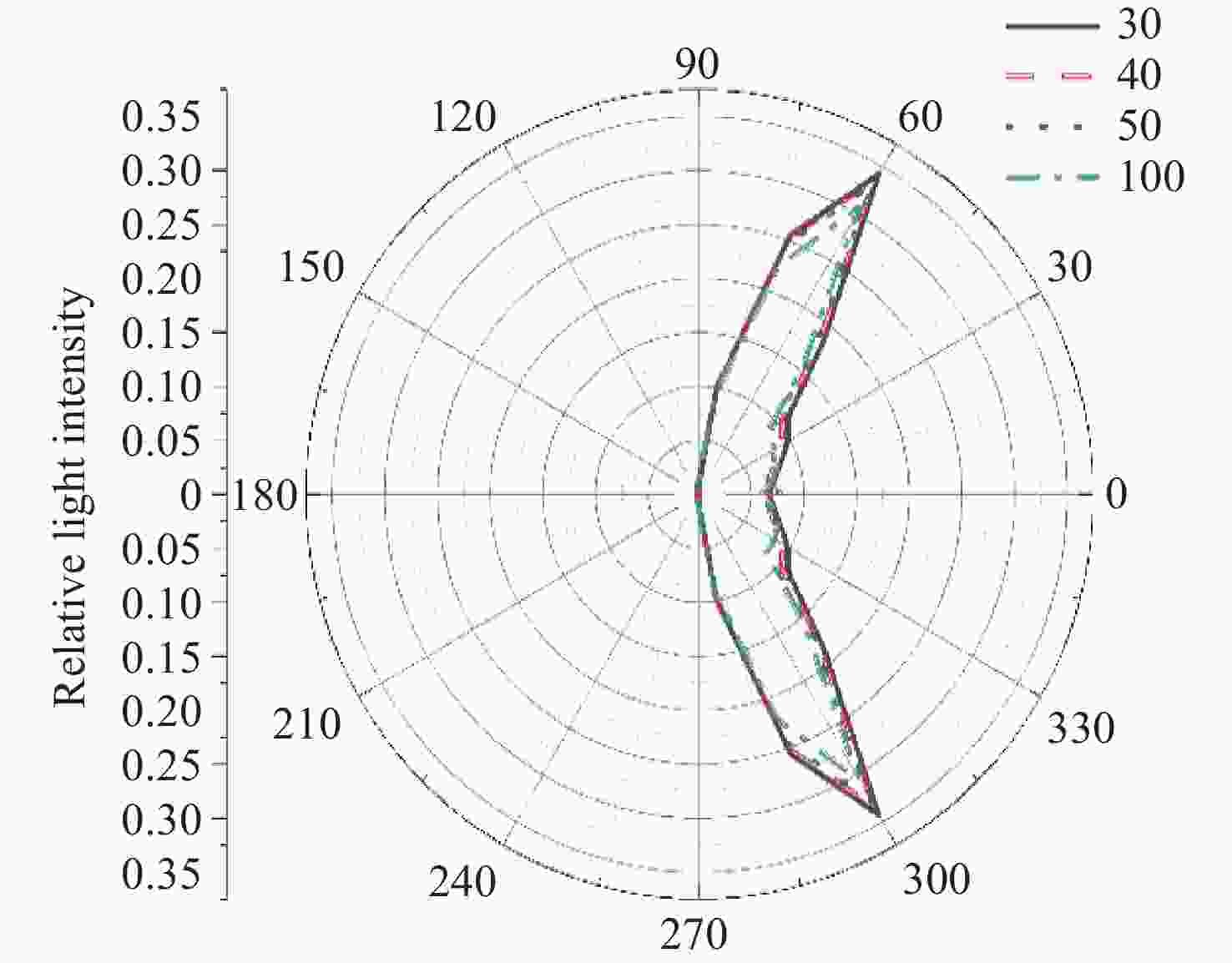
Cell size Light beam angle
without reflectionLight extraction
efficiencyNumber of
light beams30 30 0.521 2 40 30 0.505 2 50 30 0.490 2 100 30 0.456 2 Table 9. Beam angles and output efficiencies of 5050 SMT beads with a sapphire thickness of 30 μm, Al brackets, and PMMA packaging materials at an inclination angle of 85°
Diameter of
sapphire square
structureAngle of light
beam without
reflectionLight
extraction
efficiencyNumber of
light beams2 30 0.555 2 3 30 0.554 2 4 30 0.553 2 Table 10. Beam angles and output efficiencies of 5050 SMT beads with different sapphire thicknesses and Al brackets and PMMA packaging materials at an inclination angle of 85°
Sapphire length Light beam angle without reflection Light extraction efficiency Number of light beams 10 30 0.547 2 30 30 0.553 2 50 30 0.553 2 -
[1] KIKUCHI S, SHIBATA Y, ISHINABE T, et al. Thin mini-LED backlight using reflective mirror dots with high luminance uniformity for mobile LCDs[J]. Optics Express, 29(17): 26724-26735. [2] GAO ZH W, NING H L, YAO R H, et al. Mini-LED backlight technology progress for liquid crystal display[J]. Crystals, 2022, 12(3): 313. doi: 10.3390/cryst12030313 [3] YANG ZH Y, HSIANG E L, QIAN Y ZH, et al. Performance comparison between mini-LED backlit LCD and OLED display for 15.6-inch notebook computers[J]. Applied Sciences, 2022, 12(3): 1239. doi: 10.3390/app12031239 [4] ZOU G W, WANG Z Y, LIU Y T, et al. Deep learning-enabled image content-adaptive field sequential color LCDs with mini-LED backlight[J]. Optics Express, 2022, 30(12): 21044-21064. doi: 10.1364/OE.459752 [5] HSIANG E L, YANG ZH Y, YANG Q, et al. Prospects and challenges of mini-LED, OLED, and micro-LED displays[J]. Journal of the Society for Information Display, 2021, 29(6): 446-465. doi: 10.1002/jsid.1058 [6] MILLER M E. LCD Display Technology[M]//MILLER M E. Color in Electronic Display Systems: Advantages of Multi-primary Displays. Cham: Springer, 2019: 87-105. [7] ZOU G W, WANG Z Y, YANG W CH, et al. 65‐1: Deep learning-enabled image content adaptive driving algorithm for field sequential color LCDs with mini-LED backlight[J]. SID Symposium Digest of Technical Papers, 2022, 53(1): 857-860. doi: 10.1002/sdtp.15628 [8] HUANG Y G, TAN G J, GOU F W et al. Prospects and challenges of mini-LED and micro-LED displays[J]. Journal of the Society for Information Display, 2019, 27(7): 387-401. doi: 10.1002/jsid.760 [9] LEE J G, KO J H. Optimization of the optical structure of thin direct-lit LED backlights for LCD applications by using micro-LEDs[J]. Journal of Information Display, 2020, 21(1): 65-70. doi: 10.1080/15980316.2019.1693436 [10] SHEN B, ASPELL J, RINEHART T, et al. P‐206: Late-news-poster: lattice patterned micro lens array (MLA) optical films for mini-LED back light units (BLUs)[J]. SID Symposium Digest of Technical Papers, 2020, 51(1): 1649-1651. doi: 10.1002/sdtp.14211 [11] HSIANG E L, LI Y N Q, HE Z Q, et al. Enhancing the efficiency of color conversion micro-LED display with a patterned cholesteric liquid crystal polymer film[J]. Nanomaterials, 2020, 10(12): 2430. doi: 10.3390/nano10122430 [12] YU X J, XIANG L Y, ZHOU SH L, et al. Effect of refractive index of packaging materials on the light extraction efficiency of COB-LEDs with millilens array[J]. Applied Optics, 2021, 60(2): 306-311. doi: 10.1364/AO.410141 [13] HUANG C G, HU M, ZHANG CH Y, et al. Narrow beam uniform illumination design of COB light source[J]. High Power Laser and Particle Beams, 2021, 33(2): 029002. (in Chinese). [14] HAO R, GE A, TAO X, et al. Optical design of a high-mast luminaire based on four COB LED light source modules[J]. Lighting Research & Technology, 2019, 51(3): 447-456. [15] QIU Y, CHEN H H, MENG W X. Channel modeling for visible light communications—a survey[J]. Wireless Communications and Mobile Computing, 2016, 16(14): 2016-2034. doi: 10.1002/wcm.2665 [16] WANG K, CHEN F, LIU Z Y, et al. Design of compact freeform lens for application specific light-emitting diode packaging[J]. Optics Express, 2010, 18(2): 413-425. doi: 10.1364/OE.18.000413 [17] KEMPER B, STÜRWALD S, REMMERSMANN C, et al. Characterisation of light emitting diodes (LEDs) for application in digital holographic microscopy for inspection of micro and nanostructured surfaces[J]. Optics and Lasers in Engineering, 2008, 46(7): 499-507. doi: 10.1016/j.optlaseng.2008.03.007 [18] GFELLER F R, BAPST U. Wireless in-house data communication via diffuse infrared radiation[J]. Proceedings of the IEEE, 1979, 67(11): 1474-1486. doi: 10.1109/PROC.1979.11508 [19] GALEOTTI F, MRÓZ W, SCAVIA G, et al. Microlens arrays for light extraction enhancement in organic light-emitting diodes: A facile approach[J]. Organic Electronics, 2013, 14(1): 212-218. doi: 10.1016/j.orgel.2012.10.034 [20] CARRASCOSA M, CUSSO F, AGULLO-LOPEZ F. Lambert emitters: a simple Monte-Carlo approach to optical diffusers[J]. European Journal of Physics, 1985, 6(3): 183-187. doi: 10.1088/0143-0807/6/3/011 [21] WEI W, CHEN Y Y, WANG C X, et al. Simulation of far-field light distribution of micro-LED based on its structural parameters[J]. Materials, 2022, 15(24): 8854. doi: 10.3390/ma15248854 [22] FAN Z Y, LIN J Y, JIANG H X. III-nitride micro-emitter arrays: development and applications[J]. Journal of Physics D:Applied Physics, 2008, 41(9): 094001. doi: 10.1088/0022-3727/41/9/094001 [23] PARK H J, CHA Y J, KWAK J S. Chip size-dependent light extraction efficiency for blue micro-LEDs[J]. Journal of the Korean Institute of Electrical and Electronic Material Engineers, 2019, 32(1): 47-52. [24] BAYNEVA I I. Calculation and construction of optical elements of light devices[J]. Dilemas Contemp Educ Política Valores, 2019, 6: 58. [25] GUO W, MENG H, CHEN Y R, et al. Wafer-level monolithic integration of vertical micro-LEDs on glass[J]. IEEE Photonics Technology Letters, 2020, 32(12): 673-676. doi: 10.1109/LPT.2020.2991672 [26] LELIKOV Y S, BOCHKAREVA N I, GORBUNOV R I, et al. Measurement of the absorption coefficient for light laterally propagating in light-emitting diode structures with In0.2Ga0.8N/GaN quantum wells[J]. Semiconductors, 2008, 42(11): 1342-1345. doi: 10.1134/S1063782608110195 [27] ZHAO G Y, ISHIKAWA H, JIANG H, et al. Optical absorption and photoluminescence studies of n-type GaN[J]. Japanese Journal of Applied Physics, 1999, 38(9A): L993-L995. doi: 10.1143/JJAP.38.L993 [28] YANG D, THOMAS M E, TROPF W J. Infrared refractive index of sapphire as a function of temperature[J]. Proceedings of SPIE, 1999, 3705: 60-69. doi: 10.1117/12.354642 [29] O’MAHONY D, HOSSAIN M N, JUSTICE J, et al. High index contrast optical platform using gallium phosphide on sapphire: an alternative to SOI?[J]. Proceedings of SPIE, 2012, 8431: 84311H. doi: 10.1117/12.922687 [30] TRAN N T, SHI F G. LED package design for high optical efficiency and low viewing angle[C]. Proceedings of 2007 International Microsystems, Packaging, Assembly and Circuits Technology, IEEE, 2007: 10-13. -


 下载:
下载:


